Advanced electronic product designs are generally composed of multiple PCB designs that are interconnected to create a complete, functional system. From a design with a main board and a front panel LCD module to a complex active back-plane system with plug-in cards, all are implemented as a system of multiple board designs.
This requires a high-level design system that allows multiple ‘child’ PCB designs to be electrically and physically connected together while maintaining the integrity of their Pin and Net connectivity. Integrated system-level design is supported by Altium Designer in the form of a dedicated Multi-board Design environment that features both the logical (schematic) and physical (PCB) aspects of system design.
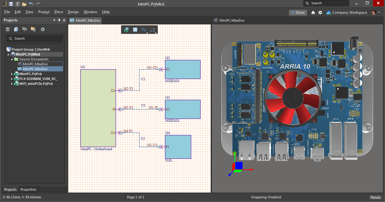
A system-level Multi-board Design is hosted in Altium Designer by a dedicated Multi-board project type (*.PrjMbd) and its constituent schematic-based logical design document (*.MbsDoc) and physical PCB-based documents (*.MbaDoc). The document types bring existing Altium Designer project designs into the Multi-board design environment where they are interconnected, edited and checked as a complete system.
The essential steps for creating a Multi-board system Schematic design from child PCB project designs are:
- Create an Altium Designer Multi-board project and add a Multi-board schematic document to the project.
- Place graphical blocks (Modules) in the Schematic to logically represent the child projects.
- Link each Module to its appropriate child project.
- Import the child project connectivity data into the system design.
- Add connections between Modules to create the logical system design.
The physical counterpart to the logical system design in a Multi-board Schematic document is a Multi-board Assembly document, which is populated with imported PCB data from the Multi-board Project. Each PCB project Module in the Multi-board system design Schematic is represented by a physical PCB in the matching Multi-board Assembly document.
► See the Multi-board Assembly documentation for information on creating and working with a Multi-board Assembly.
Enabling PCB Projects for Multi-board Design
Altium Designer PCB projects that represent the child board designs in a Multi-board system design will contain specific connections, such as edge connectors or header plugs/sockets, that are included as the electrical and physical interface to other PCBs in the system design.
These connections and their associated electrical Nets need to be detected and processed by a Multi-board schematic (logical) design document to establish the inter-board connectivity in the system-level design. This functionality is enabled by the presence of a specific component parameter for the PCB project connectors – a parameter named System, with Connector as the parameter value.
Connectors with the System:Connector Parameter:Value are detected when each system-level module is synchronized to its child PCB project using the Import from Child Projects command. This is explained in the upcoming Multi-board Schematic Design section.
For each connector in a PCB project design that is intended for a system-level interconnection, select the connector part, then add the special component parameter under the Parameters tab of the Properties panel.
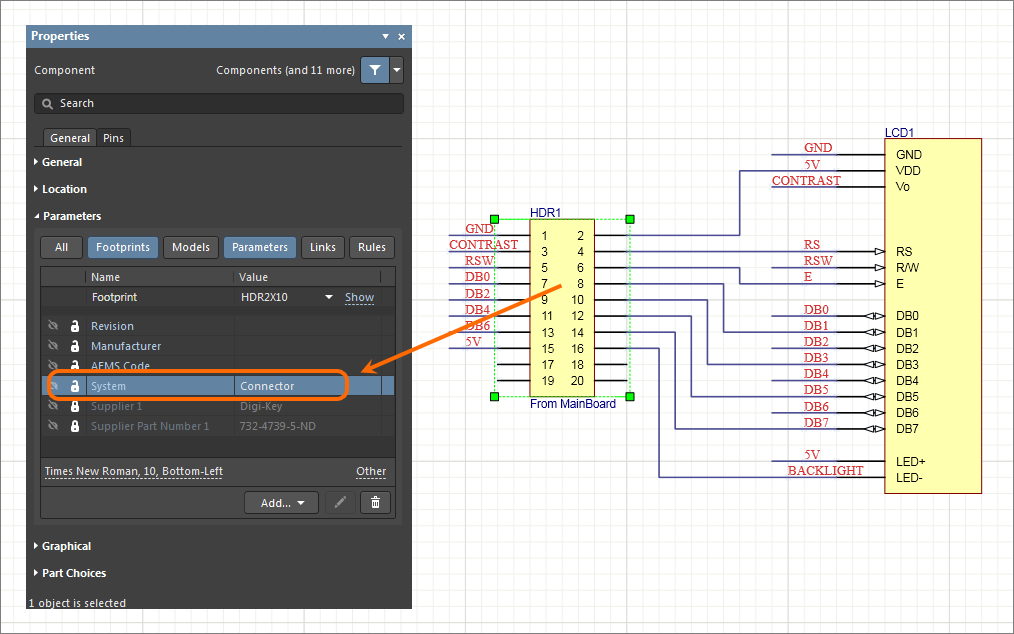 The presence of the parameter named
 System, with a value of Connector, links this PCB connector to the Multi-board schematic.
Multi-board Design Project
An Altium Designer system-level design is formed in a Multi-board project, which like any other project type is created through File » New » Project. The Create Project dialog opens; select an option under the Multiboard heading in the Project Type region.
The core design element in a Multi-board project is the logical connection design, which is developed in a Multi-board schematic document (*.MbsDoc). Add this file type to the Multi-board project from the Projects panel by right-clicking on the project entry then selecting Add New to Project » Multi-board Schematic from the context menu.
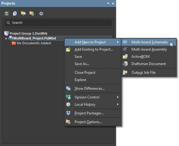
For both the Multi-board Project and its (open) schematic documents, right-click on their entries in the Projects panel then select the File » Save As option to rename the document files accordingly.
Multi-board Schematic Design
The connectivity between PCB projects that make up a Multi-board system design is established by placing representative blocks (Modules) on the schematic and connecting their exposed connectors (Entries) together using virtual connections and/or wires.
Modules, representing child PCB project designs and specific PCBs therein, are placed in the design space from the Place » Module menu or by selecting the Module button ( ) in the editor's Active Bar – see below.
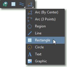 Altium Designer includes an Active Bar at the top of each editor’s workspace that provides shortcut buttons for object placement commands.
A small triangle shape in the lower area of a button indicates that a drop-down menu is available for accessing other related commands. Click and hold the button to open its menu.
To assist repeated object placement, the button icon and function will actively change to show the last used menu option.
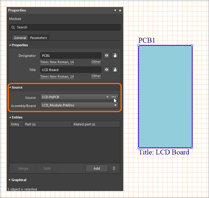
Double-click a placed Module and use the Properties panel to define its Designator and Title, and also the source PCB design project to which the Module is linked. Use the  associated with the Source field to set to a local or Workspace project, and the desired board design within that project specified (Assembly/Board).
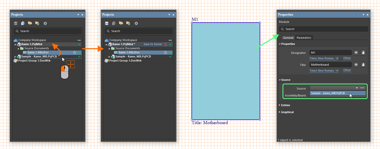
Alternatively, if a PCB project to be made a part of the multi-board project is already open, you can drag the entry of the PCB project to the multi-board project structure in the Project panel. After that, the PCB project and its PCB document can be chosen as the Source for the module selected in the multi-board schematic document.
ModuleExpandCollapse
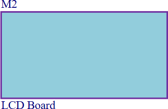
A placed Module
Summary
A Module is a rectangular object that can be placed on a multi-board Design document to represent a child PCB project design. The connectivity between PCB projects that make up a multi-board system design is established by placing modules on the schematic and connecting their exposed connectors (Module Entries) together using virtual connections, such as Wires.
Availability
Modules are available for placement in the multi-board schematic editor as follows:
- Choose the Place » Module command from the main menus.
- Click the
 button on the Active Bar located at the top of the design space.
- Right-click in the drawing design space then select Place » Module from the context menu.
Placement
After launching the command, the cursor will change to a cross-hair and the editor will enter Module placement mode. Placement is made by performing the following sequence of actions:
- Click to anchor the first corner of the Module shape.
- Move the cursor to adjust the size of the Module rectangle and click again to complete placement.
- Continue placing further Modules or right-click or press Esc to exit the placement mode.
Graphical Editing
This method of editing allows a placed Module object to be selected in the design space and graphically edit its size, shape or location.
Select a Module by clicking on its fill or outline. Once selected, editing handles/nodes are available at each corner vertex.
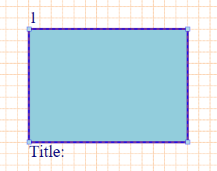
A selected Module
- Click and drag a node to reposition it and alter the size of the Module rectangle.
- Click and drag the Module object to reposition it in the schematic.
Non-Graphical Editing
Properties page: Module Properties
The non-graphical method of editing a Module is available in the multi-board Properties panel, which provides editable property fields for the item that is currently selected in the design space.
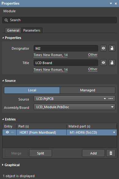 The Properties panel when a Module object is selected.
To open the Properties panel and access the properties of a placed Module:
- After selecting the Module object, select the Properties panel from the Panels button at the bottom right of the design space or select View » Panels » Properties from the main menus.
- Double-click on the Module object.
- Right-click on the Module then select Item Properties from the context menu.
If the Properties panel is already active, click on the Module to access its properties in the panel.
The Module properties can be accessed prior to entering placement mode, from the
Multi-board Schematic – Defaults page of the
Preferences dialog. This allows the default properties for the Module object to be changed, which will be applied when placing subsequent Modules.
Editing Multiple Objects
The Properties panel supports multiple object editing where the property settings that are identical in all currently selected objects may be modified. When multiples of the same object type are selected, a Properties panel field entry can be edited for all selected objects. If values of a property are different for objects in the selection, the appropriate field will be shown as an asterisk (*); a new property value will be applied to all selected objects.
Right-click Commands
A range of commands are available for quick access in the Design sub-menu when right-clicking on a Module. Note that some commands in the context menu can be accessed when a Module is not selected.
- RunERC – perform an Electrical Rules Check (ERC) on the Multi-board project design and its sources.
- Import From Child Projects – propagate the design data from all source (child) PCB projects into their specified Modules.
- Import From Selected Child Projects – propagate the design data from the corresponding source (child) PCB projects for the currently selected Module(s).
- Update Child Projects – perform an Engineering Change Order (ECO) to edit the source projects to match (synchronize to) any related changes in the Multi-board document. For example, a change to the pinout configuration of a system interconnection header/plug part.
- Update Selected Child Projects – perform an ECO to edit the source project to match any related changes in the currently selected Module.
- Update Assembly Projects – perform an ECO to edit the Multi-board PCB Assembly document to match any related changes in the Multi-board Schematic document.
- Crossprobe to PCB/Multi-board – cross probe to (open and zoom to) the selected Module’s corresponding the board layout design.
- Crossprobe to Schematic – cross probe to the selected Module’s corresponding schematic document sheet.
- Crossprobe to MBA board – cross probe to the selected Module’s corresponding board layout in the Multi-board Assembly document.
- Connection Manager – open the multi-board editor’s Connection Manager dialog.
Module PropertiesExpandCollapse
Multi-board object properties are definable options that specify the visual style, content and behavior of the placed object. The property settings for each type of object are defined in two different ways:
- Pre-placement settings – most Module object properties, or those that can logically be pre-defined, are available as editable default settings on the Multi-board Schematic - Defaults page of the Preferences dialog (access from the
 button at the top-right of the design space). Select the object in the Primitive List to reveal its options on the right.
- Post-placement settings – all Module object properties are available for editing in the Properties panel when a placed Module is selected in the design space.
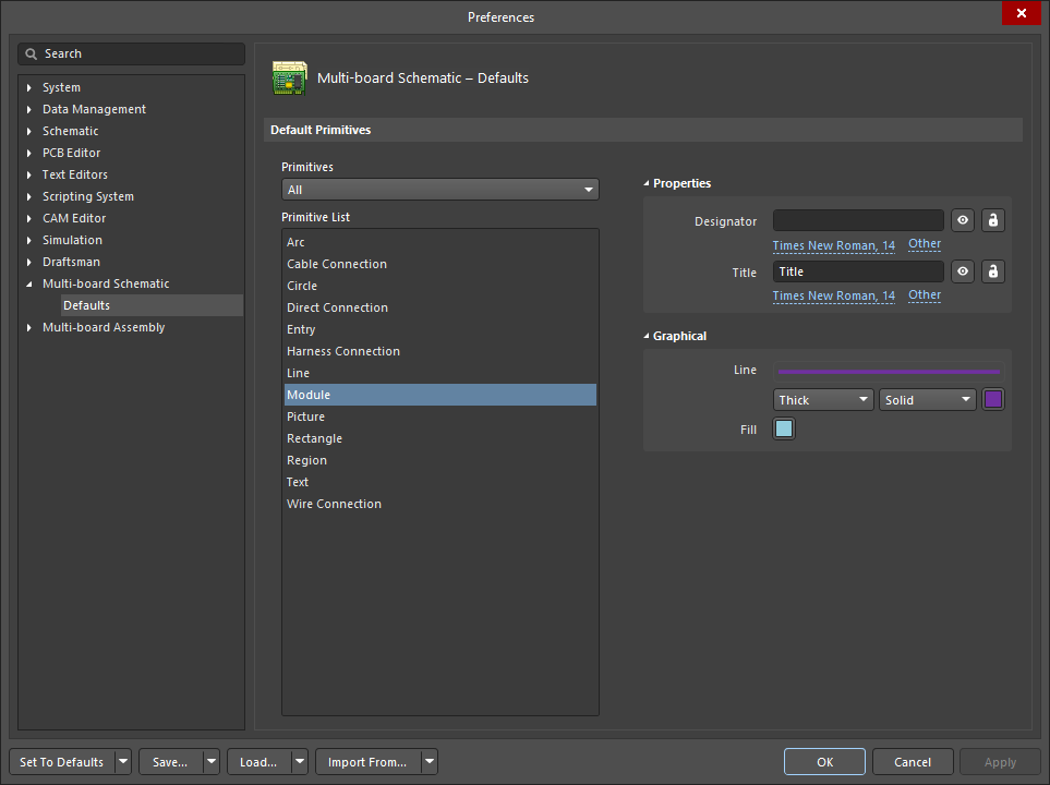
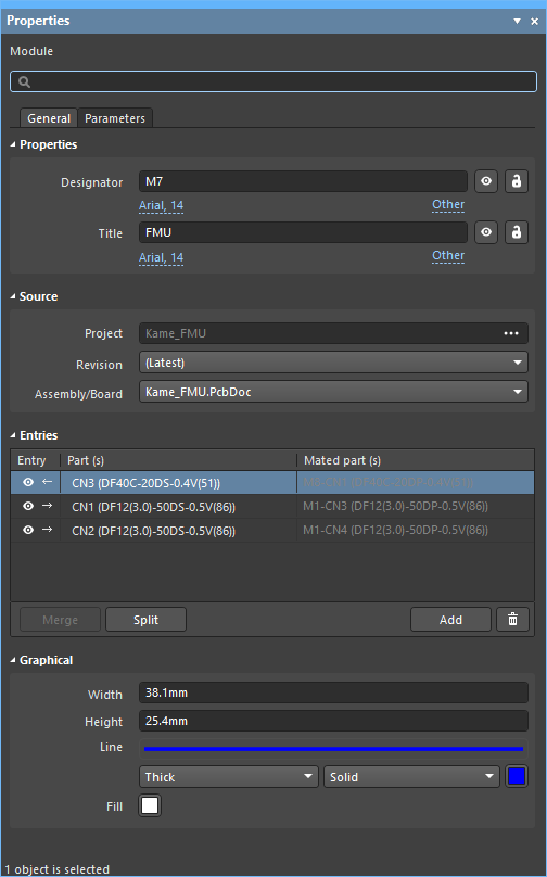 The Module object default settings in the Preferences dialog, and the Module mode of the Properties panel
In the below properties listing, options that are not available as default settings in the Preferences dialog are noted as 'Properties panel only'.
Properties
- Designator – specifies the schematic identifier for this Module.
-
 - use to toggle the designator visibility in the schematic and the
  button to toggle the value's ability to be edited.
- Font link - select to open Font Settings to edit the Designator's font, size, color, and special attributes, such as bold.
- Other - click the link to set auto-positioning (Designator at the top-left of the Module rectangle).
- Title – specifies the Module's title string.
- Use the
 button to toggle its visibility in the schematic and the
  button to toggle the value's ability to be edited.
- Select the font link to access and edit the Title's font settings, attributes and color. Select the Other link to set auto-positioning (Title at the bottom-left), and the visibility of the parameter name ('Title').
Source (Properties panel only)
This section defines the source PCB design project to which the Module is linked. Click the  button to the right of the Source field to open the
 ![]() Choose Project dialog, from where you can choose the required PCB project - either a local project or a project managed within your connected Workspace. Once chosen, click Open - the panel will refresh with the fields applicable to that type of project:
Choose Project dialog, from where you can choose the required PCB project - either a local project or a project managed within your connected Workspace. Once chosen, click Open - the panel will refresh with the fields applicable to that type of project:
- Local
- Source – the PCB project.
- Assembly/Board – the board design within that source project. If there are multiple PCB documents, select the desired board from the drop-down menu.
- Managed
- Project – the chosen source PCB project, resident within your connected Workspace.
- Revision – select the required revision of the assembly of the source managed project that will apply to the multi-board Module. By default, the latest release will be selected.
- Assembly/Board – the board design within that source managed project. If there are multiple PCB documents, select the desired board from the drop-down menu.
Entries (Properties panel only)
The Entries section is a tabular list of the connectors registered with the selected Module and the connectors to which they are mated on other Modules. The list is populated when a connector Entry has been added to the Module – see Multi-board Schematic design for more information.
- Entry column – sets the visual attributes of the Entry on the schematic. Use the
 button to toggle its visibility and the
  button to toggle its connector type – male/female.
- Part column – the Designator and Name of the Entry connector in the source PCB design. This can be edited for convenience – the naming is local to the Multi-board system design and does not affect the source Child Projects.
- Mated part column – the name of the part, such as a header, on a Module to which the Entry is connected by a Wire or Direct Connection, etc.
Use the buttons in the the lower area of the region to manage and edit the Entries in the list.
-
 – unites previously split Entries back into their single Entry version – see below.
-
 – divides the selected connection in the list into two related Module Entries where the Pins/Nets to be separated off into the new Entry are nominated in the Split Entry dialog. See Split Connections for more information.
-
 – adds a new undefined Entry to the Module and list.
-
 – remove the selected Entry in the list from the Module.
Add further modules and their child project links to the multi-board schematic design, as required for the complete system design.
The Modules are populated with design data from their linked PCB project designs by importing the project data using the Design » Import From Child Projects command or the Design » Import From Selected Child Projects command. Most importantly, this processes the Pin and Net data from each connector in the Child Projects that have the special System:Connector parameter (i.e. parameter named System with a value of Connector) attached.
After the import is complete, a module Entry is automatically created for each of these connectors on their respective Module block graphic. The connector Entry is actively associated with Pins and Nets on the connector in the Child Project.
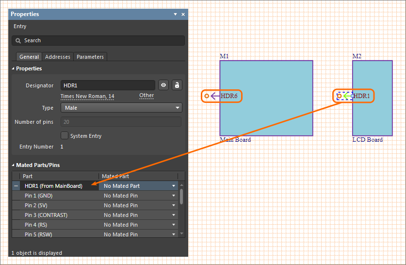
Select an
Entry graphic in the workspace to see its details, such as its connector Pins/Nets, in the
Properties panel. Until connected to the Entry on another module, the Entry's Part/Pin listing in the panel will show the connector and pins as not mated.
Module EntryExpandCollapse
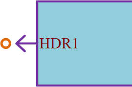
A Module Entry on a placed Module.
Summary
A Module Entry is a graphical object that is automatically or manually placed on Module in a Multi-board Design document to represent a connection point (such as a header or plug/socket) of a child PCB project design. Module Entries are connected to entries on other Modules using virtual connections, such as Wires. A Module Entry can also represent a terminating connector of a cable or harness connection that mates to a board connector.
Availability
Module Entries are available for placement in the multi-board schematic editor as follows:
- Choose the Place » Entry command from the main menu.
- Click the
 button on the Active Bar located at the top of the design space.
- Right-click in the drawing design space then select Place » Entry from the context menu.
The most common way that an Entry is added to a Module is when its associated child project data is imported (Import From Child Project). The addition is an automated process, where the multi-board editor detects valid system connectors in the Module's child project then adds Entries to the Module that represent those connectors.
Placement
After launching the command, the Module Entry graphic will be attached to the cursor, ready for placement. Then:
- Hover the cursor over the target Module to locate a suitable position and click to complete placement.
- Continue placing further Entries or right-click or press Esc to exit the placement mode.
The coloring of the entry will aid in its correct placement. While outside of a module, the entry will be partially presented and appear grayed out, and you will be prevented from placing it. When over a module, the full (and colored) entry will appear, indicating it can be placed at that location.
Graphical Editing
This method of editing allows a placed Module Entry object to be selected in the design space and graphically edit its location.
Select a Module by clicking on its graphic then drag the Entry around the Module's perimeter to a suitable location. Note that the Entry name can be independently dragged to a different position.
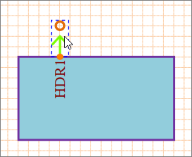
A selected Module Entry
You can move a group of module entries by selecting more than one entry and then dragging the group to the desired location, as shown in the video below.
Non-Graphical Editing
Properties page: Module Entry Properties
The non-graphical method of editing a Module Entry is available in the Multi-board Properties panel, which provides editable property fields for the item that is currently selected in the design space.
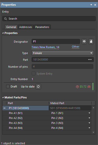 The Properties panel when a Module Entry object is selected.
To open the Properties panel and access the properties of a placed Module Entry:
- After selecting the Module Entry object, select the Properties panel from the Panels button at the bottom right of the design space or select View » Panels » Properties from the main menus.
- Double-click on the Module Entry object.
- Right-click on the Module Entry then select Item Properties from the context menu.
If the Properties panel is already active, click on the Module Entry to access its properties in the panel.
The Module Entry properties can be accessed prior to entering placement mode, from the
Multi-board Schematic – Defaults page of the
Preferences dialog. This allows the default properties for the Module Entry object to be changed, which will be applied when placing subsequent Module Entries.
Editing Multiple Objects
The Properties panel supports multiple object editing where the property settings that are identical in all currently selected objects may be modified. When multiples of the same object type are selected, a Properties panel field entry can be edited for all selected objects. If values of a property are different for objects in the selection, the appropriate field will be shown as an asterisk (*); a new property value will be applied to all selected objects.
Module Entry PropertiesExpandCollapse
Multi-board object properties are definable options that specify the visual style, content and behavior of the placed object. The property settings for each type of object are defined in two different ways:
- Pre-placement settings – most Module Entry object properties, or those that can logically be pre-defined, are available as editable default settings on the Multi-board Schematic - Defaults page of the Preferences dialog (access from the
 button at the top-right of the design space). Select the object in the Primitive List to reveal its options on the right.
- Post-placement settings – all Module Entry object properties are available for editing in the Properties panel panel when a placed Module Entry is selected in the design space.
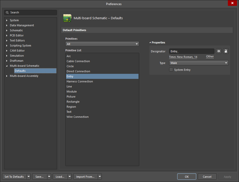
 The Entry object default settings in the Preferences dialog, and the Entry mode of the Properties panel.
In the below properties listing, options that are not available as default settings in the Preferences dialog are noted as 'Properties panel only'.
Properties
Mated Parts/Pins (Properties panel only)
The Mated Parts/Pins region lists the physical part represented by the Entry and connection to which it mates, such as a Wire. Select the  symbol to expand the list for access to part's Pin to connector wire/pin mapping.
- Part column – in expanded view, a list of the individual pins in the connector part and their associated net.
- Mated part column – the corresponding list of the Connector entries to which each Part pin is connected, such as an individual wire.
Addresses tab (Properties panel only)
Provides a tabular listing of the connection paths and nets for the selected Module Entry.
- From Name column – the part, pin and net name of the source connection in the Entry's Module.
- To Name column – the part, pin and net name of the terminating connection in the 'target' Module.
- Net Name column – the net name for the connection as either a single name or as an aggregated net name (
target_net/source_net).
Parameters tab (Properties panel only)
Parameters that are associated with a Module Entry are accessed under the Parameters tab of the Properties panel. All other properties are accessed under the default General tab.
- Name – the Parameter Name of the listed parameter entry.
- Value – the Parameter Value associated with the listed parameter Name.
- Options
- Use the
 button to toggle a Parameter's visibility in the schematic and the
  button to toggle its ability to be edited.
- Select the font link (e.g.,
Times New Roman...) to access and edit the Parameter's font settings, attributes and color. Select the Other option to set auto-positioning (Parameter at the bottom of the Module Entry rectangle) and the visibility of the Parameter Name.
- Add/Delete – click
 to add a new default Parameter entry to the list. Click
  to remove the selected Parameter from the list.
Project Structure
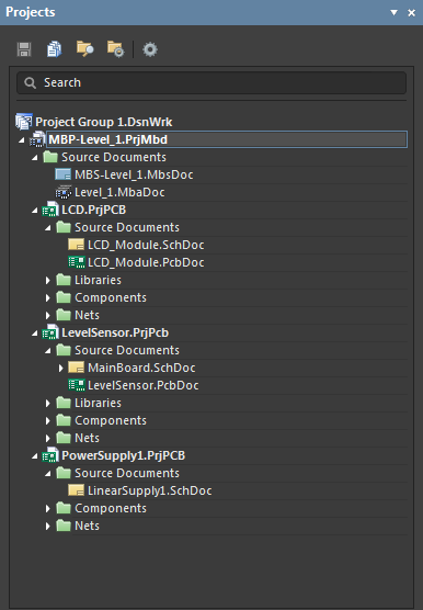
An established Multi-board Project features a hierarchical document structure that includes Source documents (Multi-board Schematic and Assembly), and the child PCB sub-projects linked to Modules in the schematic system design. The structure of a child project is immediately added to the Multi-board Project when a system design Module has been linked to that external project.
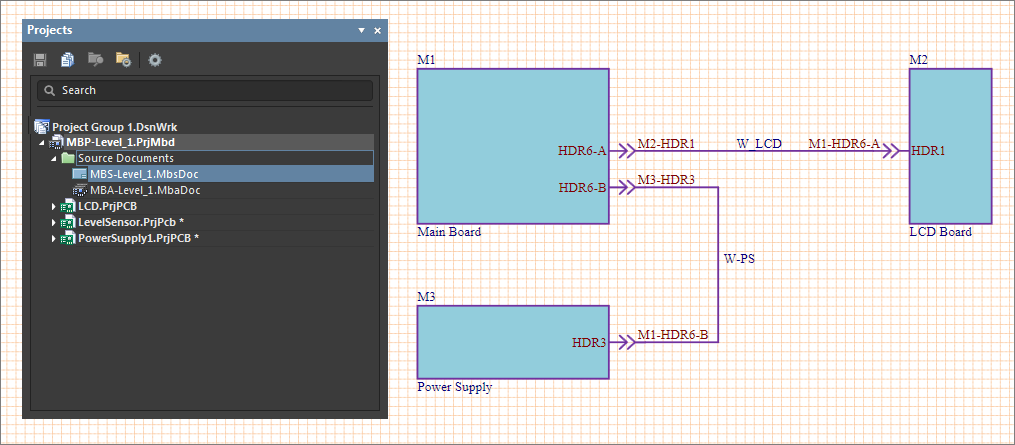
Expand the project structure in the Projects panel to expose the constituent files in the multi-board project and its child projects. To ensure that the Multi-board project extracts and processes the correct data from its sub-projects, the PCB of each project should be synchronized with its Schematic and free of design or drafting errors. To validate a sub-project, right-click on its name in the panel and select the Validate PCB Project <name> command – any issues will be listed in the Messages panel.
Cross-Probing
- To cross-probe from the currently selected module or entry to the top-level schematic or connector on the relevant schematic within the PCB design project referenced by that module, use the Design » Crossprobe to Schematic command from the main menus or context menu of the design space.
- To cross-probe from the currently selected module or entry to the PCB document or connector on that document within the PCB design project referenced by that module, use the Design » Crossprobe to PCB/Multi-board command from the main menus or context menu of the design space. If the module references a Multi-board Assembly document (*.MbaDoc) within a source Multi-board project (*.PrjMbd), then cross-probing will be to the Multi-board Assembly document.
- To cross-probe from the currently selected module or entry to the board, or connector on that board, on the Multi-board Assembly document (*.MbaDoc) within the Multi-board project (*.PrjMbd), use the Design » Crossprobe to MBA command from the main menus or context menu of the design space.
- To cross-probe from the currently selected harness connection on the multi-board schematic document (*.MbsDoc) to a linked harness project (
*.PrjHar), use the Design » Crossprobe to Harness command from the main menus or right-click menu in the design space. The wiring diagram document of the associated harness project will open.
When cross-probing from a module entry, the cross-probed object(s) on the target schematic/PCB document will be displayed in accordance with the
Highlight Methods options defined on the
System - Navigation page of the
Preferences dialog. Highlighting will not be applied to the Multi-board Schematic document.
Graphical Objects
The multi-board schematic editor provides a range of graphical element tools that can be used to place basic, free-form drawing elements in a multi-board schematic sheet. For information on multi-board schematic editor graphical objects, and their associated settings in the Properties panel, refer to the collapsible sections below:
ArcExpandCollapse
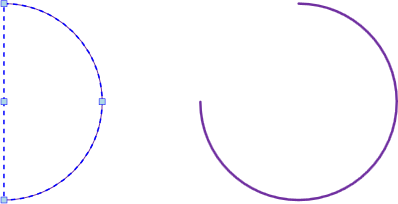 Two placed Arcs; the one on the left is in edit mode.
Summary
An Arc is a graphic object that can be placed on a multi-board Design schematic document and set to the desired arc angle, radius and line style. An Arc can be placed using a center or three-point method.
Availability
An arc can be placed in the multi-board schematic editor in the following ways:
- Choose the Place » Arc (By Center) or Place » Arc (3 Points) command from the main menu.
- Click the
 or
or  button in the graphic objects drop-down on the Active Bar located at the top of the design space. Click and hold an Active Bar button to access other related commands. Once a command has been used, it will become the topmost item on that section of the Active Bar.
- Right-click in the drawing design space then select Place » Arc (By Center) or Place » Arc (3 Points) from the context menu.
Placement
After launching either command, the cursor changes to a cross-hair indicating Arc placement mode.
Arc by Center placement steps:
- Click to set the center point of the arc.
- Move the cursor to adjust the radius and starting point of the arc then click to confirm.
- Move the cursor to set the end point (and total angle) of the arc then click to confirm.
- Continue placing further arcs or right-click or press Esc to exit arc placement mode.
Arc in 3 Points placement steps:
- Click to set the starting point of the arc (point #1).
- Move the cursor to set the end point of the arc then click to confirm (point #2).
- Move the cursor to set the radius of the arc then click to confirm (point #3).
- Continue placing further arcs or right-click or press Esc to exit arc placement mode.
Graphical Editing
This method of editing allows a placed Arc object to be selected in the design space and then graphically edit its location, radius and start/end points.
Select an Arc by clicking on its outline. Once selected, editing handles/nodes are available at its center, perimeter and start/end points:
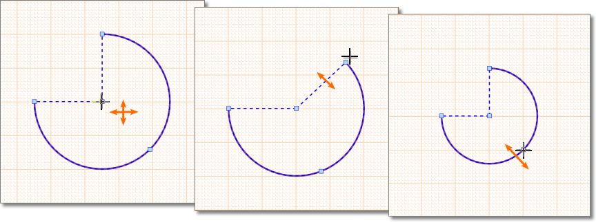 The ways in which Arc nodes may be manipulated.
- Click and drag the arc's center node to reposition it on the drawing document.
- Click and drag a start or end point node to alter the arc angle.
- Click and drag the perimeter node to change the radius of the arc.
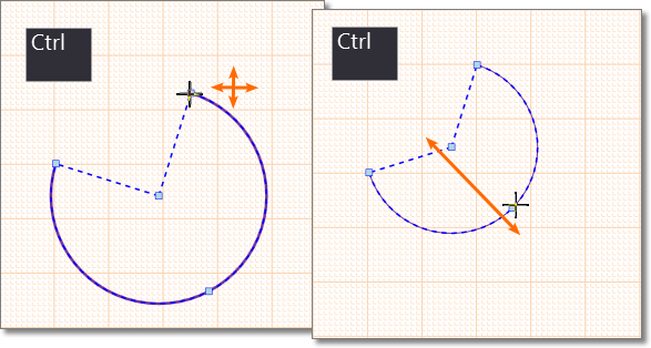
Advanced manipulation of an Arc is available by pressing the Ctrl key while moving an editing node:
- Click and drag a start or end point node to alter its location while retaining the arc angle.
- Click and drag the perimeter node to alter the size of the arc while retaining its start and end points.
Non-Graphical Editing
Properties page: Arc Properties
The non-graphical method of editing an Arc is available in the Properties panel, which provides editable property fields for the item that is currently selected in the design space.
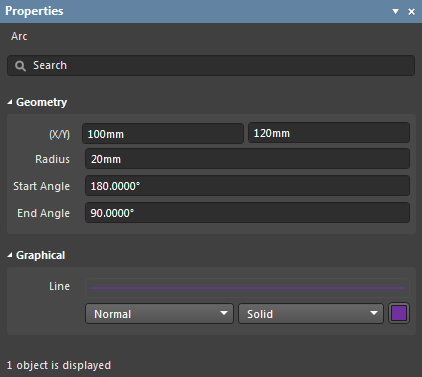 The Properties panel when an Arc object is selected.
To open the Properties panel and access the properties of a placed Arc:
- After selecting the Arc object, select the Properties panel from the Panels button at the bottom right of the design space or select View » Panels » Properties from the main menus.
- Double-click on the Arc's perimeter.
- Right-click on the Arc perimeter then select Item Properties from the context menu.
If the Properties panel is already active, click on the Arc's perimeter to access its properties in the panel.
The Arc properties can be accessed prior to entering placement mode, from the
Multi-board Schematic – Defaults page of the
Preferences dialog. This allows the default properties for the Arc object to be changed, which will be applied when placing subsequent Arcs.
Editing Multiple Objects
The Properties panel supports multiple object editing where the property settings that are identical in all currently selected objects may be modified. When multiples of the same object type are selected, a Properties panel field entry can be edited for all selected objects. If values of a property are different for objects in the selection, the appropriate field will be shown as an asterisk (*); a new property value will be applied to all selected objects.
Arc PropertiesExpandCollapse
Multi-board object properties are definable options that specify the visual style, content and behavior of the placed object. The property settings for each type of object are defined in two different ways:
- Pre-placement settings – most Arc object properties, or those that can logically be pre-defined, are available as editable default settings on the Multi-board Schematic - Defaults page of the Preferences dialog (access from the
 button at the top-right of the design space). Select the object in the Primitive List to reveal its options on the right.
- Post-placement settings – all Arc object properties are available for editing in the Properties panel when a placed Arc is selected in the design space.
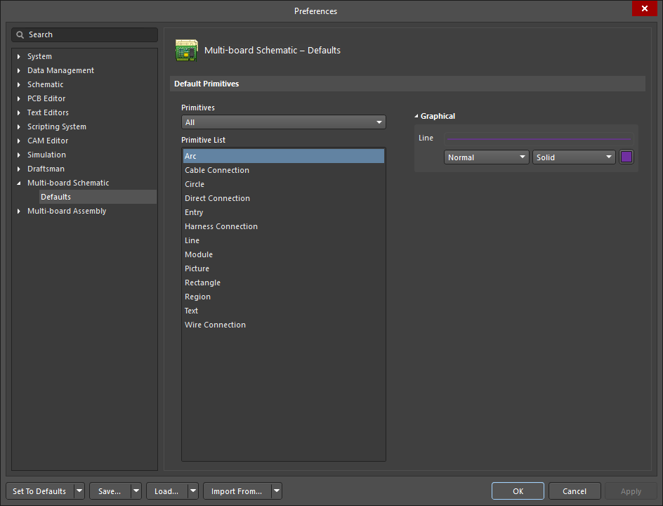
 The Arc object default settings in the Preferences dialog and the Arc mode of the Properties panel.
In the below properties listing, options that are not available as default settings in the Preferences dialog are noted as; 'Properties panel only'.
Geometry (Properties panel only)
- (X/Y) – the X-axis and Y-axis values of the arc's center point relative to the document origin.
- Radius – the radius (center to perimeter distance) of the selected Arc.
- Start Angle – the angle of the Arc start point relative to the arc center in the X-axis.
- End Angle – the angle of the Arc end point relative to the arc center in the X-axis.
Graphical
- Line – displays the Arc's current outline weight/style/color.
- Line weight – use to define the line thickness. Use the drop-down to choose from a range of line weight presets.
- Line pattern – use to define the pattern style applied to line. Use the drop-down to choose from a range of line style presets.
- Line color (
 ) – click to open the line color selector, which includes options for preset colors, HEX/RGB color values, the graphic selection of color shades, and variable color opacity.
CircleExpandCollapse
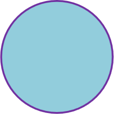 A placed Circle
Summary
A Circle is a graphic object that can be placed on a Multi-board Design schematic document and filled with a specified solid color.
Availability
Circles are available for placement in the multi-board schematic editor as follows:
- Choose the Place » Circle command from the main menu.
- Click the
 button in the graphic objects drop-down on the Active Bar located at the top of the design space. Click and hold an Active Bar button to access other related commands. Once a command has been used, it will become the topmost item on that section of the Active Bar.
- Right-click in the drawing design space then select Place » Circle from the context menu.
Placement
After launching the command, the cursor will change to a cross-hair and the editor will enter circle placement mode. Placement is made by performing the following actions:
- Click to define the center position of the circle.
- Move the cursor to adjust the radius of the circle then click again to complete placement.
- Continue placing further circles or right-click or press Esc to exit the placement mode.
Graphical Editing
This method of editing allows a placed circle object to be selected in the design space and graphically edit its radius or location.
Select a Circle by clicking on its fill or outline. Once selected, editing handles/nodes are available at its center and perimeter.
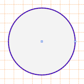 A selected Circle
- Click and drag the Circle's center node to reposition it on the drawing document.
- Click and drag a perimeter node to alter the Circle radius.
Non-Graphical Editing
Properties page: Circle Properties
The non-graphical method of editing a Circle is available in the Multi-board Properties panel, which provides editable property fields for the item that is currently selected in the design space.
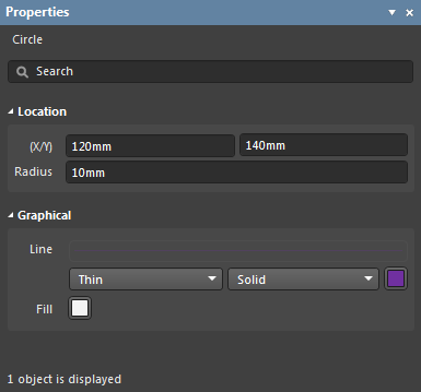 The Properties panel when a Circle object is selected.
To open the Properties panel and access the properties of a placed Circle:
- After selecting the Circle object, select the Properties panel from the Panels button at the bottom right of the design space or select View » Panels » Properties from the main menus.
- Double-click on the Circle object.
- Right-click on the Circle then select Item Properties from the context menu.
If the Properties panel is already active, click on the Circle to access its properties in the panel.
The Circle properties can be accessed prior to entering placement mode, from the
Multi-board Schematic – Defaults page of the
Preferences dialog. This allows the default properties for the Circle object to be changed, which will be applied when placing subsequent Circles.
Editing Multiple Objects
The Properties panel supports multiple object editing where the property settings that are identical in all currently selected objects may be modified. When multiples of the same object type are selected, a Properties panel field entry can be edited for all selected objects. If values of a property are different for objects in the selection, the appropriate field will be shown as an asterisk (*); a new property value will be applied to all selected objects.
Circle PropertiesExpandCollapse
LineExpandCollapse
 A placed Line
Summary
A Line is a graphic object that can be placed on a multi-board Design schematic document.
Availability
Lines are available for placement in the multi-board schematic editor as follows:
- Choose the Place » Line command from the main menu.
- Click the
 button in the graphic objects drop-down on the Active Bar located at the top of the design space. Click and hold an Active Bar button to access other related commands. Once a command has been used, it will become the topmost item on that section of the Active Bar.
- Right-click in the drawing design space then select Place » Line from the context menu.
Placement
After launching the command, the cursor will change to a cross-hair and the editor will enter Line placement mode. Placement is made by performing the following actions:
- Click to define the starting position of the Line.
- Move the cursor to set the length and angle the Line then click again to complete placement.
- Continue placing further Lines or right-click or press Esc to exit the placement mode.
Graphical Editing
The graphical method of editing allows a placed Line object to be selected in the design space and moved or its start/end point locations changed.
When a Line object is selected, editing handles/nodes become available at its start and end points.
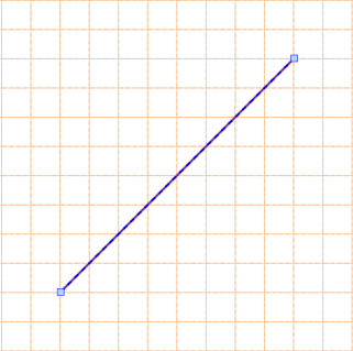 A selected Line. Click and drag the Line to reposition it on the drawing document.
- Click and drag a start or finish point node to alter the Line's position, angle or length.
Non-Graphical Editing
Properties page: Line Properties
The non-graphical method of editing a Line is available in the Multi-board Properties panel, which provides editable property fields for the item that is currently selected in the design space.
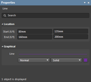 The Properties panel when a Line object is selected.
To open the Properties panel and access the properties of a placed Line:
- After selecting the Line object, select the Properties panel from the Panels button at the bottom right of the design space or select View » Panels » Properties from the main menus.
- Double-click on the Line object.
- Right-click on the Line then select Item Properties from the context menu.
If the Properties panel is already active, click on the Line to access its properties in the panel.
The Line properties can be accessed prior to entering placement mode, from the
Multi-board Schematic – Defaults page of the
Preferences dialog. This allows the default properties for the Line object to be changed, which will be applied when placing subsequent Lines.
Editing Multiple Objects
The Properties panel supports multiple object editing where the property settings that are identical in all currently selected objects may be modified. When multiples of the same object type are selected, a Properties panel field entry can be edited for all selected objects. If values of a property are different for objects in the selection, the appropriate field will be shown as an asterisk (*); a new property value will be applied to all selected objects.
Line PropertiesExpandCollapse
Multi-board object properties are definable options that specify the visual style, content and behavior of the placed object. The property settings for each type of object are defined in two different ways:
- Pre-placement settings – most Line object properties, or those that can logically be pre-defined, are available as editable default settings on the Multi-board Schematic - Defaults page of the Preferences dialog (access from the
 button at the top-right of the design space). Select the object in the Primitive List to reveal its options on the right.
- Post-placement settings – all Line object properties are available for editing in the Properties panel when a placed Line is selected in the design space.
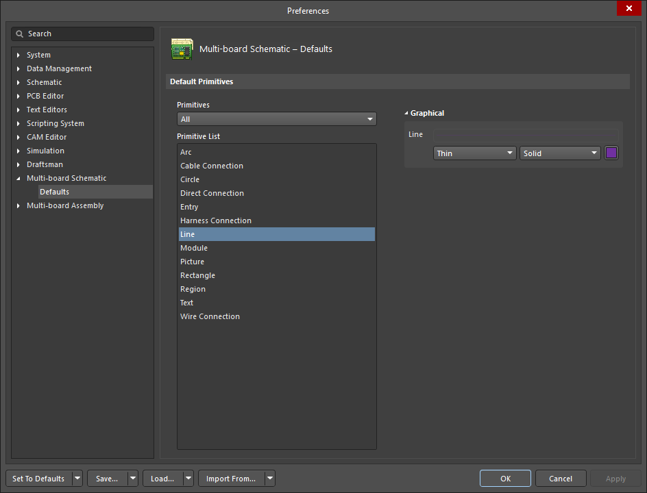
 The Line object default settings in the Preferences dialog, and the Line mode of the Properties panel
In the below properties listing, options that are not available as default settings in the Preferences dialog are noted as 'Properties panel only'.
Location (Properties panel only)
- Start (X/Y) – the X-axis and Y-axis values of the Line's start point (the first point placed).
- End (X/Y) – the X-axis and Y-axis values of the Line's end point.
Graphical
- Line – displays and sets the Line graphic's weight/style/color
- Line weight – the line thickness. Use the drop-down menu to choose from a range of line weight presets.
- Line pattern – the pattern style applied to Line. Use the drop-down menu to choose from a range of line style presets.
- Line color (
 ) – click to open the Line color selector drop-down, which includes options for preset colors, HEX/RGB color values and the graphic selection of color shades.
PictureExpandCollapse
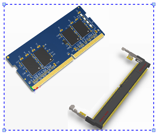 A placed and selected Picture box object
Summary
A Picture object is an image container that can be placed on a multi-board Design schematic document and populated with a standard image file (*.png, *.jpeg, *.jpg, *.jpe, *.jfif, *.gif, *.bmp).
Availability
An Image container object is available for placement in the multi-board schematic editor as follows:
- Choose the Place » Graphic command from the main menu.
- Click the
 button in the graphic objects drop-down on the Active Bar located at the top of the design space. Click and hold an Active Bar button to access other related commands. Once a command has been used, it will become the topmost item on that section of the Active Bar.
- Right-click in the drawing design space then select Place » Graphic from the context menu.
Placement
After launching the command, the cursor will change to a cross-hair and the editor will enter the Picture container placement mode. Placement is made by performing the following sequence of actions:
- Click to define the first corner position of the Picture box.
- Move the cursor to adjust the size of the box (and opposite corner position) then click again to complete placement.
- Select a suitable image from the file browser.
If the
Maintain Aspect Ratio option is checked in the
Properties panel (the default setting), move one of the Picture box editing nodes to sync the box aspect ratio to that of the source image.
Graphical Editing
This method of editing allows a placed Picture object to be selected in the design space and then graphically edit its size or location.
When a Picture object is selected, editing handles/nodes are available at each corner.
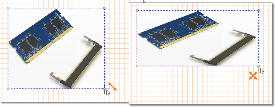 A selected Picture object is resized by dragging an editing node. If the aspect ratio is not locked, the image can be distorted to any shape.
- Click and drag on any part of the graphic object to reposition it on the document.
- Click and drag a node to alter the size of the picture container – the displayed image will automatically resize to fit. If the Maintain Aspect Ratio option is unchecked in the Properties panel, the container size can be set to dimensions that do not match the image file aspect ratio.
Non-Graphical Editing
Properties page: Picture Properties
The non-graphical method of editing a Picture container object is available in the multi-board Properties panel, which provides editable property fields for the item that is currently selected in the design space.
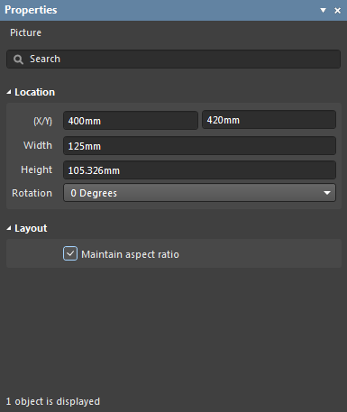 The Properties panel when a Picture object is selected.
To open the Properties panel and access the properties of a placed Picture object:
- After selecting the Picture object, select the Properties panel from the Panels button at the bottom right of the design space or select View » Panels » Properties from the main menus.
- Double-click on the Picture object.
- Right-click on the Picture object then select Item Properties from the context menu.
If the Properties panel is already active, click on the Picture object to access its properties in the panel.
The Picture properties can be accessed prior to entering placement mode, from the
Multi-board Schematic – Defaults page of the
Preferences dialog. This allows the default properties for the Picture object to be changed, which will be applied when placing subsequent Pictures.
Editing Multiple Objects
The Properties panel supports multiple object editing where the property settings that are identical in all currently selected objects may be modified. When multiples of the same object type are selected, a Properties panel field entry can be edited for all selected objects. If values of a property are different for objects in the selection, the appropriate field will be shown as an asterisk (*); a new property value will be applied to all selected objects.
Picture PropertiesExpandCollapse
Multi-board object properties are definable options that specify the visual style, content and behavior of the placed object. The property settings for each type of object are defined in two different ways:
- Pre-placement settings – most Picture object properties, or those that can logically be pre-defined, are available as editable default settings on the Multi-board Schematic - Defaults page of the Preferences dialog (access from the
 button at the top-right of the design space). Select the object in the Primitive List to reveal its options on the right.
- Post-placement settings – all Picture object properties are available for editing in the Properties panel when a placed Picture object is selected in the design space.
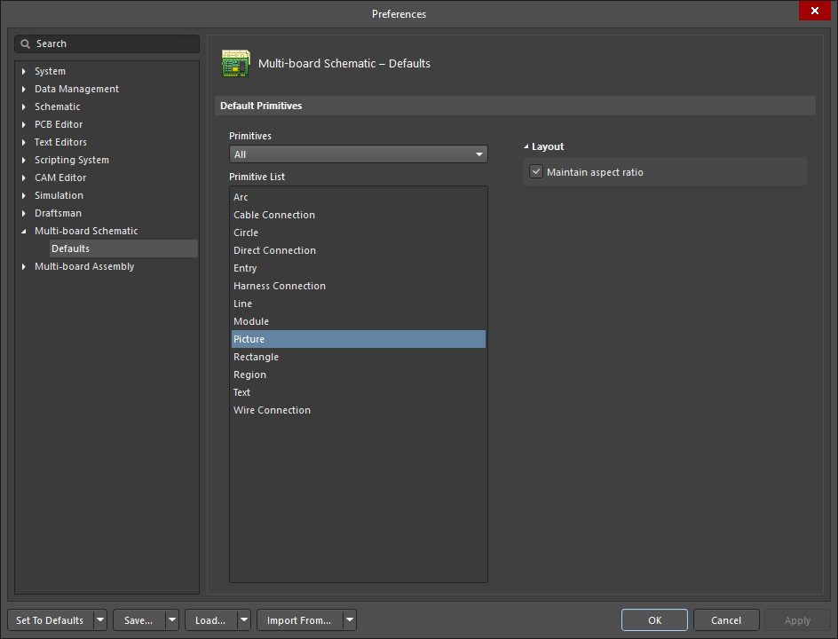
 The Picture object default settings in the Preferences dialog and the Picture mode of the Properties panel
In the below properties listing, options that are not available as default settings in the Preferences dialog are noted as 'Properties panel only'.
Location (Properties panel only)
- (X/Y) – the X-axis and Y-axis values of the Picture container's reference location (bottom-left corner position).
- Width – the (X-axis) width of the selected Picture object.
- Height – the (Y-axis) height of the selected Picture object. This is determined by the aspect ratio of the contained image file when the Maintain aspect ratio option is enabled (see below).
- Rotation – the horizontal/vertical orientation of the Picture box. Use the drop-down to select from: 0 degrees, 90 degrees, 180 degrees, 270 degrees.
Layout
- Maintain aspect ratio – when checked, the X/Y dimensions of the Picture container will scale in proportion to the aspect ratio of the source image. The source image will always fill the Picture container.
RectangleExpandCollapse
 A placed Rectangle
Summary
A Rectangle is a graphic object that can be placed on a multi-board Design schematic document and filled with a specified solid color.
Availability
Rectangles are available for placement in the Multi-board schematic editor as follows:
- Choose the Place » Rectangle command from the main menus.
- Click the
 button in the graphic objects drop-down on the Active Bar located at the top of the design space. Click and hold an Active Bar button to access other related commands. Once a command has been used, it will become the topmost item on that section of the Active Bar.
- Right-click in the drawing design space then select Place » Rectangle from the context menu.
Placement
After launching the command, the cursor will change to a cross-hair and the editor will enter Rectangle placement mode. Placement is made by performing the following actions:
- Click to anchor the first corner of the rectangle.
- Move the cursor to adjust the size of the rectangle and click again to complete placement.
- Continue placing further Rectangles or right-click or press Esc to exit the placement mode.
Graphical Editing
This method of editing allows a placed Rectangle object to be selected in the design space and graphically edit its size, shape or location.
Select a Rectangle by clicking on its fill or outline. Once selected, editing handles/nodes are available at its center and perimeter.
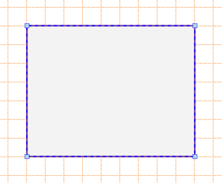 A selected Rectangle
- Click and drag a node to reposition it and alter the size of the Rectangle.
- Click and drag the rectangle object to reposition the rectangle in the schematic.
Non-Graphical Editing
Properties page: Rectangle Properties
The non-graphical method of editing a Rectangle is available in the Multi-board Properties panel, which provides editable property fields for the item that is currently selected in the design space.
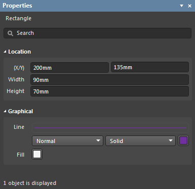 The Properties panel when a Rectangle object is selected.
To open the Properties panel and access the properties of a placed Rectangle:
- After selecting the Rectangle object, select the Properties panel from the Panels button at the bottom right of the design space or select View » Panels » Properties from the main menus.
- Double-click on the Rectangle object.
- Right-click on the Rectangle then select Item Properties from the context menu.
If the Properties panel is already active, click on the Rectangle to access its properties in the panel.
The Rectangle properties can be accessed prior to entering placement mode, from the
Multi-board Schematic – Defaults page of the
Preferences dialog. This allows the default properties for the Rectangle object to be changed, which will be applied when placing subsequent Rectangles.
Editing Multiple Objects
The Properties panel supports multiple object editing where the property settings that are identical in all currently selected objects may be modified. When multiples of the same object type are selected, a Properties panel field entry can be edited for all selected objects. If values of a property are different for objects in the selection, the appropriate field will be shown as an asterisk (*); a new property value will be applied to all selected objects.
Rectangle PropertiesExpandCollapse
RegionExpandCollapse
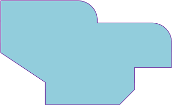 A placed Region
Summary
A Region is a closed shape object that can be placed on a Multi-board Design document to indicate a specific area in the schematic. The Region object shape can include angle-based curved lines.
Availability
Regions are available for placement in the multi-board schematic editor as follows:
- Choose the Place » Region command from the main menu.
- Click the
 button in the graphic objects drop-down on the Active Bar located at the top of the design space. Click and hold an Active Bar button to access other related commands. Once a command has been used, it will become the topmost item on that section of the Active Bar.
- Right-click in the drawing design space then select Place » Region from the context menu.
Placement
After launching the command, the cursor will change to a cross-hair and the editor will enter Region placement mode. Placement is made by performing the following sequence of actions:
- Click to place the first vertex of the Region shape.
- Move the cursor and click to place the second vertex of the Region shape.
- Continue to place further region vertices to complete the Region shape.
- After the final vertex is placed, right-click or press Esc to complete the Region shape back to the first-placed vertex.
Straight lines will be drawn between each vertex as they are placed, however the Shift+Spacebar shortcut can be used to cycle through other line options such as a 90° corner, 45° corner, curved 90° corner or curved 45° corner – this applies to the line segment between the cursor and the previously placed vertex. Once an option is selected, use the Spacebar to toggle the direction of the corner.
Graphical Editing
This method of editing allows a placed Region object to be selected in the design space and graphically edit its size, shape or location.
Select a Region by clicking on its fill or outline. Once selected, editing handles/nodes are available at each of the shape's verticess.
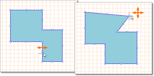 A selected Region shape is edited by dragging line or vertex nodes.
- Drag (click+hold+move) any part of the Region, but not a node, to reposition it on the document.
- Drag the center mark of a line segment to move that line in the perpendicular (maintaining its angle) to a new location.
- Drag a corner vertex node to move it to a new location and alter the Region shape.
- Ctrl+drag on a line, but not its center mark, to add a new node.
- Press Delete while dragging a node to delete it from the shape.
Non-Graphical Editing
Properties page: Region Properties
The non-graphical method of editing a Region is available in the multi-board Properties panel, which provides editable property fields for the item that is currently selected in the design space.
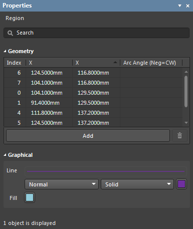 The Properties panel when a Region object is selected.
To open the Properties panel and access the properties of a placed Region:
- After selecting the Region object, select the Properties panel from the Panels button at the bottom right of the design space or select View » Panels » Properties from the main menus.
- Double-click on the Region object.
- Right-click on the Region then select Item Properties from the context menu.
If the Properties panel is already active, click on the Region to access its properties in the panel.
The Region properties can be accessed prior to entering placement mode, from the
Multi-board Schematic – Defaults page of the
Preferences dialog. This allows the default properties for the Region object to be changed, which will be applied when placing subsequent Regions.
Editing Multiple Objects
The Properties panel supports multiple object editing where the property settings that are identical in all currently selected objects may be modified. When multiples of the same object type are selected, a Properties panel field entry can be edited for all selected objects. If values of a property are different for objects in the selection, the appropriate field will be shown as an asterisk (*); a new property value will be applied to all selected objects.
Region PropertiesExpandCollapse
Multi-board object properties are definable options that specify the visual style, content and behavior of the placed object. The property settings for each type of object are defined in two different ways:
- Pre-placement settings – most Region object properties, or those that can logically be pre-defined, are available as editable default settings on the Multi-board Schematic - Defaults page of the Preferences dialog (access from the
 button at the top-right of the design space). Select the object in the Primitive List to reveal its options on the right.
- Post-placement settings – all Region object properties are available for editing in the Properties panel when a placed Region is selected in the design space.
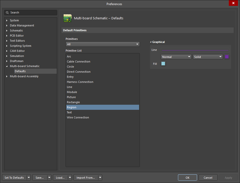
 The Region object default settings in the Preferences dialog, and the Region mode of the Properties panel
In the below properties listing, options that are not available as default settings in the Preferences dialog are noted as 'Properties panel only'.
Geometry (Properties panel only)
- Geometry – a tabular list of each vertex (node) in the Region shape in their placed order including their (X/Y) locations and associated line arc angles. Each entry may be manually edited to update the rendered Region shape. The table's Arc Angle column (if applicable) defines the curve radius of the vertex connection line from that node to the next. When edited, the resulting curve shape corresponds to the arc segment of an equivalent circle through the specified angle. Enter a negative angle to invert the arc curve.
- Add – click to duplicate the selected vertex entry. A new vertex will be inserted (in the same location) into the Region shape.
-
 – click to remove the selected vertex from the Region shape.
Graphical
- Line – displays and sets the outline weight/style/color.
- Line weight – the line thickness of the Region outline. Use the drop-down menu to choose from a range of line weight presets.
- Line pattern – the pattern line style of the Region outline. Use the drop-down menu to choose from a range of line style presets.
- Line color (
 ) – click to open the outline color selector drop-down, which includes options for preset colors, HEX/RGB color values and the graphic selection of color shades.
- Fill (
 ) – click to open the fill color selector drop-down, which includes options for preset colors, HEX/RGB color values and the graphic selection of color shades.
TextExpandCollapse
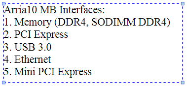 A placed and selected Text box object
Summary
A Text object is a text container object that can be placed on a multi-board Design schematic document. The text string that will be displayed in the object is entered through the Properties panel.
Availability
A Text container box is available for placement in the multi-board schematic editor as follows:
- Choose the Place » Text command from the main menu.
- Click the
 button in the graphic objects drop-down on the Active Bar located at the top of the design space. Click and hold an Active Bar button to access other related commands. Once a command has been used, it will become the topmost item on that section of the Active Bar.
- Right-click in the drawing design space then select Place » Text from the context menu.
Placement
After launching the command, the cursor will change to a cross-hair and the editor will enter text box placement mode. Placement is made by performing the following actions:
- Click to define the first corner position of the Text box.
- Move the cursor to adjust the size of the box (and opposite corner position) and then click again to complete placement.
- Continue placing further text boxes, or right-click or press Esc to exit the placement mode.
Graphical Editing
This method of editing allows a placed Text object to be selected in the design space and graphically edit its size, shape or location.
Select a Text box object by clicking on its constituent text. Once selected, editing handles/nodes are available at its perimeter.
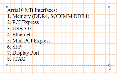 A selected Text box being resized.
- Click and drag a node to reposition it and alter the size of the Text. The text lines will automatically wrap to remain contained by the box if the Clip to Bounds option is checked in the Properties panel.
- Click and drag the text within the Text box object to reposition the box in the schematic.
Non-Graphical Editing
Properties page: Text Properties
The non-graphical method of editing a Text box and its constituent text string is available in the Multi-board Properties panel, which provides editable property fields for the item that is currently selected in the design space.
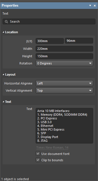 The Properties panel when a Text object is selected.
To open the Properties panel and access the properties of a placed Text box:
- After selecting the Text object, select the Properties panel from the Panels button at the bottom right of the design space or select View » Panels » Properties from the main menus.
- Double-click on the text in the Text object box.
- Right-click on the Text object then select Item Properties from the context menu.
If the Properties panel is already active, click on the text in the Text box to access its properties in the panel.
The Text properties can be accessed prior to entering placement mode, from the
Multi-board Schematic – Defaults page of the
Preferences dialog. This allows the default properties for the Text object to be changed, which will be applied when placing subsequent Texts.
Editing Multiple Objects
The Properties panel supports multiple object editing where the property settings that are identical in all currently selected objects may be modified. When multiples of the same object type are selected, a Properties panel field entry can be edited for all selected objects. If values of a property are different for objects in the selection, the appropriate field will be shown as an asterisk (*); a new property value will be applied to all selected objects.
Text PropertiesExpandCollapse
Multi-board object properties are definable options that specify the visual style, content and behavior of the placed object. The property settings for each type of object are defined in two different ways:
- Pre-placement settings – most Text object properties, or those that can logically be pre-defined, are available as editable default settings on the Multi-board Schematic - Defaults page of the Preferences dialog (access from the
 button at the top-right of the design space). Select the object in the Primitive List to reveal its options on the right.
- Post-placement settings – all Text object properties are available for editing in the Properties panel when a placed Text object is selected in the design space.
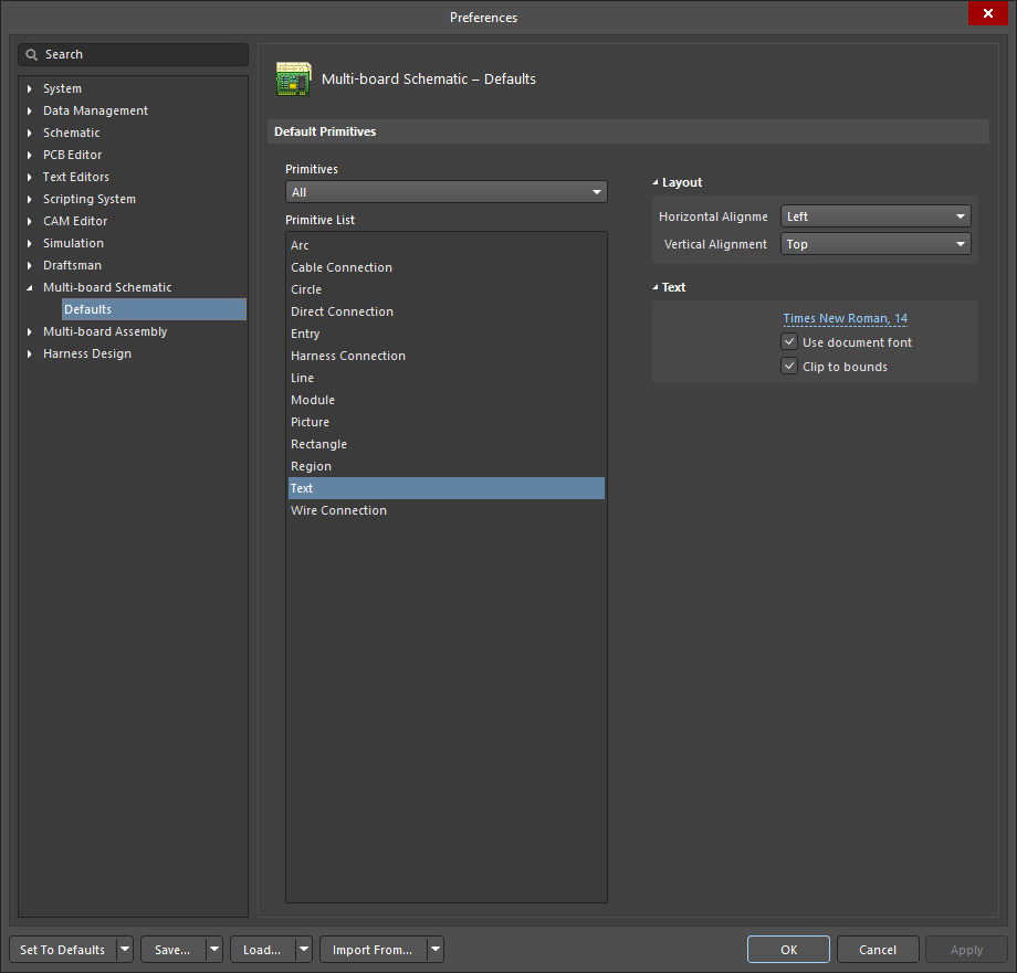
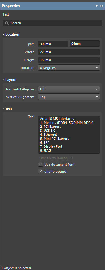
The Text object default settings in the Preferences dialog and the Text mode of the Properties panel
In the below properties listing, options that are not available as default settings in the Preferences dialog are noted as 'Properties panel only'.
Location (Properties panel only)
- (X/Y) – the X-axis and Y-axis values of the Text box reference location (bottom-left corner position).
- Width – the (X-axis) width of the selected Text box.
- Height – the (Y-axis) height of the selected Text box.
- Rotation – the horizontal/vertical orientation of the Text box. Use the drop-down menu to select from: 0 Degrees, 90 Degrees, 180 Degrees, 270 Degrees.
Layout
- Horizontal Alignment – use the drop-down menu options (
Left, Center and Right) to set the horizontal text alignment and positioning within the Text box.
- Vertical Alignment – use the drop-down menu options (
Top, Center and Bottom) to set the vertical text alignment and positioning within the Text box.
Text
- Text (Properties panel only) – the target field for the text string(s) that will appear in the displayed Text box object. Press Shift+Enter to add a new line.
- Use document font – when selected, the font style used in the Text box is that defined by the document options. See the Document Font entry in General section of the Properties panel when in Document Options mode (no schematic objects selected).
When the Use document font option is not selected (unchecked), the font used in the Text box is determined by the object font style settings. These are accessed by clicking the font style link (e.g., Times New Roman, 14) and choosing the desired font type, size, color, and text attributes from the drop-down options window.
- Font link - click this link to access the Font Settings, where you may choose the desired font type, size, and color. You may also bolden, italicize, underline, and strike-out the text. All options selected will be reflected in the font link.
- Clip to bounds – when selected, the text strings will be wrapped automatically to remain constrained within the Text box perimeter.
Print or Export to PDF
To print the currently active Multi-board Schematic document, select File » Print from the main menu (or Ctrl+P). The Print dialog will open. The left-hand side of the dialog features a scalable print preview image. If the multi-board schematic document to be printed contains multiple pages, the arrow buttons below the preview image allow you to navigate through the various pages and view them in the preview area. Standard printing options are available on the right-hand side of the dialog. These include the ability to designate a specific printer, confirm the printer's location, view how many documents are currently in the printing queue, adjust the number of copies to print, page sizing, and orientation options. After clicking Print, the print set will be sent to the chosen printing device, in accordance with the options defined.
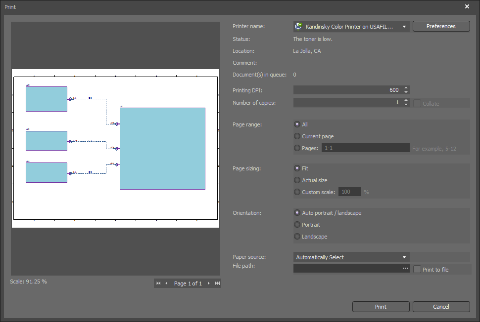
The Print dialog
To export a Multi-board Schematic document to a PDF file, select File » Export to PDF from the main menu.