Configuring the Layer Stack for Controlled Impedance Routing
This document is no longer available beyond version 21. Information can now be found here: Configuring the PCB for Controlled Impedance Routing for version 24
When the Routing Becomes Part of the Circuit
As device switching speeds increase, so too do the demands on the printed circuit board designer and the fabricator. As the length of the signal switching edge becomes shorter than the length of the PCB trace that carries it, the trace has to be treated as part of the circuit. That trace has an impedance, which is referred to as the characteristic impedance (Zo).
The best way to manage the impact of these additional circuit elements is to design the trace routing so that the characteristic impedance is consistent over the length - a technique called controlled impedance routing.
The impedance of the trace routing is defined by the:
- Cross-sectional area of the trace - determined from the width, the height (copper thickness), and the slope of the trace edges created during the etching process.
- Distance from the trace to the reference plane(s) - the return path of the signal energy is as important as the signal's path, this return path follows the signal path in the adjacent reference plane(s).
- Properties of the surrounding materials - the energy in the signal is not contained within the copper of the trace, due to the skin effect it also travels down the dielectric material that surrounds the trace. The permittivity of the dielectric material gives a measure of how much the dielectric impacts on the flow of that energy.
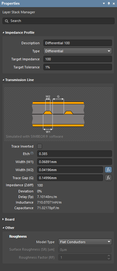 The Simbeor impedance calculator calculates the width(s) required to achieve the specified impedance.
Calculating the Impedance
In a traditional PCB design, the designer specifies the width/clearance of the trace to satisfy the current/voltage requirements.
In a controlled impedance design the designer specifies the impedance rather than the trace width. Using the built-in Simbeor® impedance calculator, the PCB editor's Layer Stack Manager calculates the trace width needed to deliver the specified impedance.
The Simbeor SFS
Impedances are calculated by the Simbeor SFS, a quasi-Static Field Solver. Simbeor SFS is an advanced quasi-static 2D field solver based on Method of Moments, which has been validated by convergence, comparisons, and measurements. The solver meshes dielectric and conductor boundaries and solves corresponding equations to build frequency-dependent RLGC matrices for the Telegraph equations.
Simbeor SFS is not a full-wave solver as this is not needed to evaluate the impedance, delay, or attenuation in PCB interconnects, because of the quasi-TEM nature of the waves propagating there. Such waves can be accurately simulated with RLGC parameters extracted with a quasi-static 2D field solver.
A unique property of the Simbeor SFS solver is that it supports conductor roughness models. Note that it does not support a multi-layered conductor model (plating), and the roughness is common for all conductors. The solver is quasi-static because the solution does not include the high-frequency dispersion that takes place in microstrip lines (higher concentration of fields in a dielectric with higher dielectric constant at high frequencies).
► Learn more about Simberian electromagnetic signal integrity technology
Supported PCB Structures
Impedances can be calculated for the following PCB structures:
- Microstrip
- Symmetrical Stripline
- Asymmetrical Stripline
- Single and differential coplanar structures
- Multiple adjacent dielectric layers, with different dielectric properties.
Creating and Configuring an Impedance Profile
The trace width required to deliver a specific impedance is calculated as part of the impedance profile, configured in the Impedance tab of the Layer Stack Manager.
Based on:
- The values of the Target Impedance, Target Tolerance and Roughness that you configure in the Impedance tab, and
- the materials settings defined in the Stackup tab, including:
- the thickness of the signal layer,
- the thickness of the surrounding dielectric layers (the distances from the reference plane(s)), and
- the properties of the dielectric material (permittivity Dk, and dissipation factor Df).
When these are correctly configured, the impedance calculator has sufficient information to calculate the:
- Trace Width
- Calculated Impedance (Z)
- Impedance Deviation (Z Deviation)
- Propagation Delay (Tp)
- Inductance per unit length (p.u.l.)
- Capacitance per unit length (p.u.l.)
The calculated values are displayed in the Transmission Line section of the Properties panel, when the Impedance tab is selected in the Layer Stack Manager, as shown below.
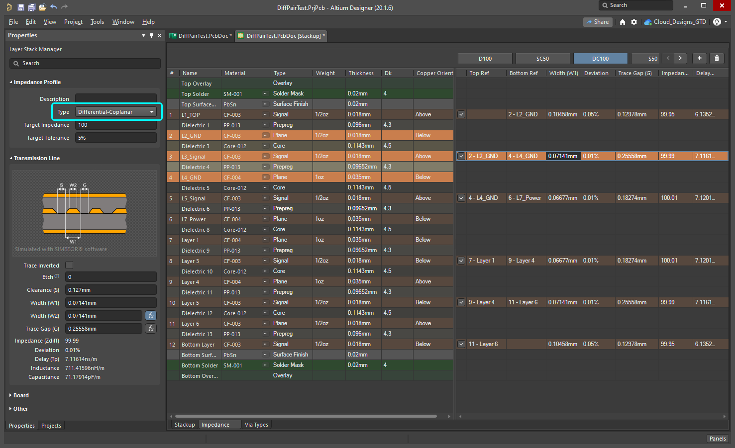
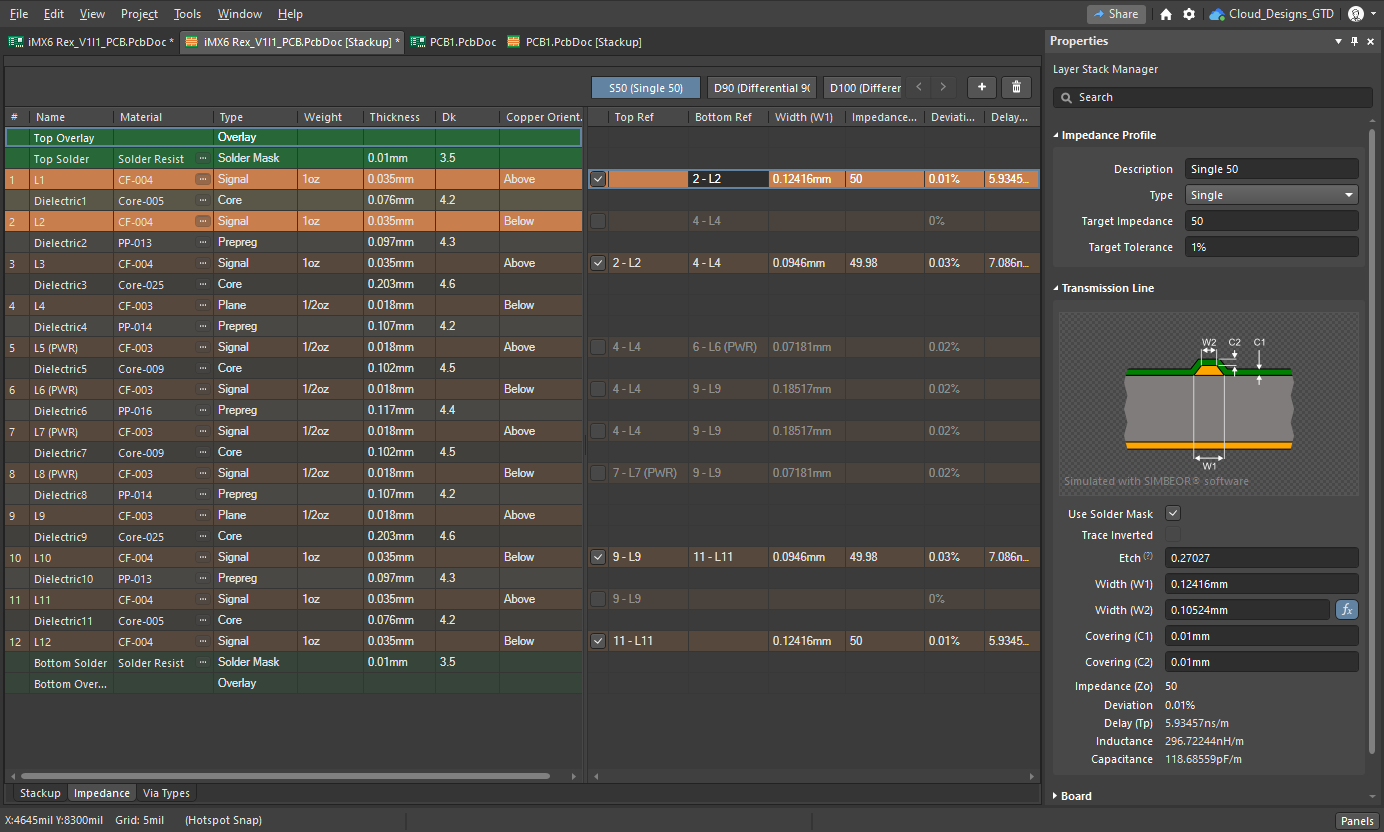 A 50Ω impedance profile defined for single nets routed on the top layer, hover the cursor over the image to display the settings for the same profile for layer L3.
(image courtesy FEDEVEL Open Source, www.fedevel.com).
Adding a new Impedance Profile
- In the Layer Stack Manager switch to the Impedance tab, as shown above.
- Click the
 button (or the
  button if there are profiles defined already), to add a new profile.
 - Define the required impedance Type, Target Impedance, and Target Tolerance in the Properties panel. The Description is optional, it will be displayed wherever the Impedance Profile name is displayed.
- The grid of layers is divided into 2 regions; the layers in the stackup are displayed on the left, then for each signal layer in the stackup there is a layer displayed in the Impedance Profile region on the right. Use the layer checkbox in the Profile region to enable impedance calculation for that layer. Using the image above as an example and referring to the layer number shown in the left-most column, layers
L1,L3,L10andL12have their layer checkbox ticked, enabling them for impedance calculations. - When you click on an enabled layer in the Profile region, all layers in the layer stack will fade except those being used to calculate the impedance for that selected signal layer (as shown in the image above). Edit that layer's reference layer(s) in the Top Ref and Bottom Ref columns in the Impedance Profile region. Note that reference layer(s) can have a layer Type of either
Planeor Signal. For example, in the image above, layerL10in the stackup is enabled for impedance calculations, with the Top Ref set to9-L9, which is aPlanelayer, and the Bottom Ref set to11-L11, which is a Signal layer. The software assumes that if a signal layer is being used as a reference plane, it contains a continuous plane of copper connected to a power or ground net. - Enable the Impedance Profile checkbox for each other layer that will carry routing at this impedance, and configure the reference plane(s). Hover the cursor over the image above to display the S50 Impedance Profile for layer
L3.
Tuning the Width and Gap Settings
From the target impedance and target tolerance, the software calculates the Trace Width. It is not uncommon that the calculated trace width will be a value that cannot be ordered, for example 0.0683mm. The fabricator will advise what material thicknesses are available and what precision they can achieve for trace widths. Then it becomes a process of starting at the desired values, then testing the impact on the calculated impedance values when the dimensions are adjusted to what is available.
To support this process of testing and tuning the settings, the impedance calculators support forward and reverse impedance calculations. The default mode is forward (enter the impedance, the software calculates the width). The  icon indicates the calculated variable.
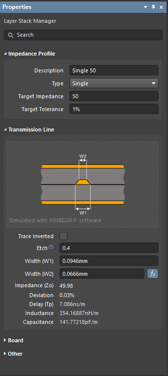
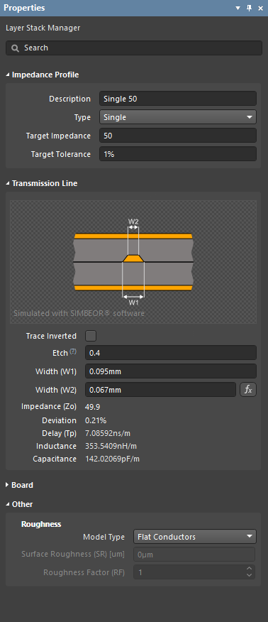
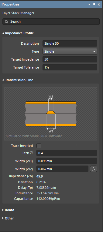 A Target Impedance of 50Ω gives a forward calculated width (W1) of 94.6µm, the image on the right shows the reverse calculation when the width (W1) is set to 95µm.
To reverse the calculation and explore different trace widths for the selected layer, type in the new Width (W1) value and press Enter on the keyboard. The calculated values will update to reflect the impact of changing to that width. Click the  button to return the calculator to forward calculation mode. Entering a new value into Width (W2) will change the Etch value.
To explore the differential pair transmission line results, nominate the calculated variable - either the Trace Width or Trace Gap - by clicking the appropriate  button. Edit the other variable to change the Target Impedance, or alternatively change the Target Impedance to explore the impact on the other variable.
Etch Factor
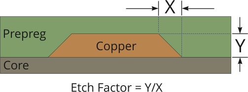
The signal traces on a PCB are fabricated by etching away unwanted copper. Because the etchant starts etching away the copper at the surface, this copper spends more time in contact with the etchant. The result is the finished edges of the trace will have a slope, reducing the cross-sectional area of the finished trace, as shown in the image below.
The area of trace-edge copper lost (on both edges) during etching = X * Y
The amount of slope is referred to as the Etch Factor, where:
Etch Factor = Y/X
If Y = X, then the Etch Factor = 1
Referring to the image shown in the Properties panel:
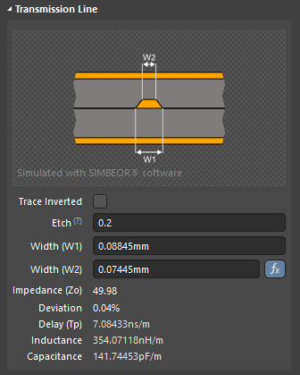 Hover the cursor over the ? to show the formula.
The standard definition for Etch Factor is to specify it as the ratio of trace thickness / amount of over-etching. This gives the following formula:
Etch Factor = T/[0.5(W1-W2)]
The downside of this approach is that to specify no over-etching (meaning the trace edges are vertical), you would have to enter a value of inf (infinite) for the etch factor. To simplify specifying the amount of etch, the formula has been inverted so a value of 0 (zero) can be entered to indicate there is no over-etching.
Etch = [0.5(W1-W2)]/T
Copper orientation
Another fabrication detail that contributes to the etch factor is the orientation of the copper. PCB traces are formed by etching away unwanted copper from a continuous sheet of copper laminated onto a dielectric substrate. The copper orientation defines the direction the copper projects away from that substrate. You can also think of it as the direction the copper is etched from, either above or below.
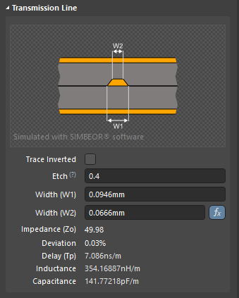
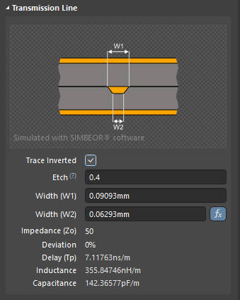 Click the Trace Inverted checkbox to toggle the Copper Orientation from Above to Below.
Conductor Surface Roughness
The surface of each of the copper layers in a printed circuit board has a degree of roughness. During PCB fabrication the surface of copper layers are treated to increase the roughness, to improve the adhesion between the copper and dielectric layers. This surface roughness becomes a significant contributor to conductor impedance at switching speeds above 10 GB/s. Through extensive research and analysis, industry experts have concluded that the surface roughness can be modeled by a roughness correction coefficient, derived from Surface Roughness and Roughness Factor values.
Roughness settings are available in the Layer Stack Manager mode of the Properties panel. These parameters are used only for conductive layers.
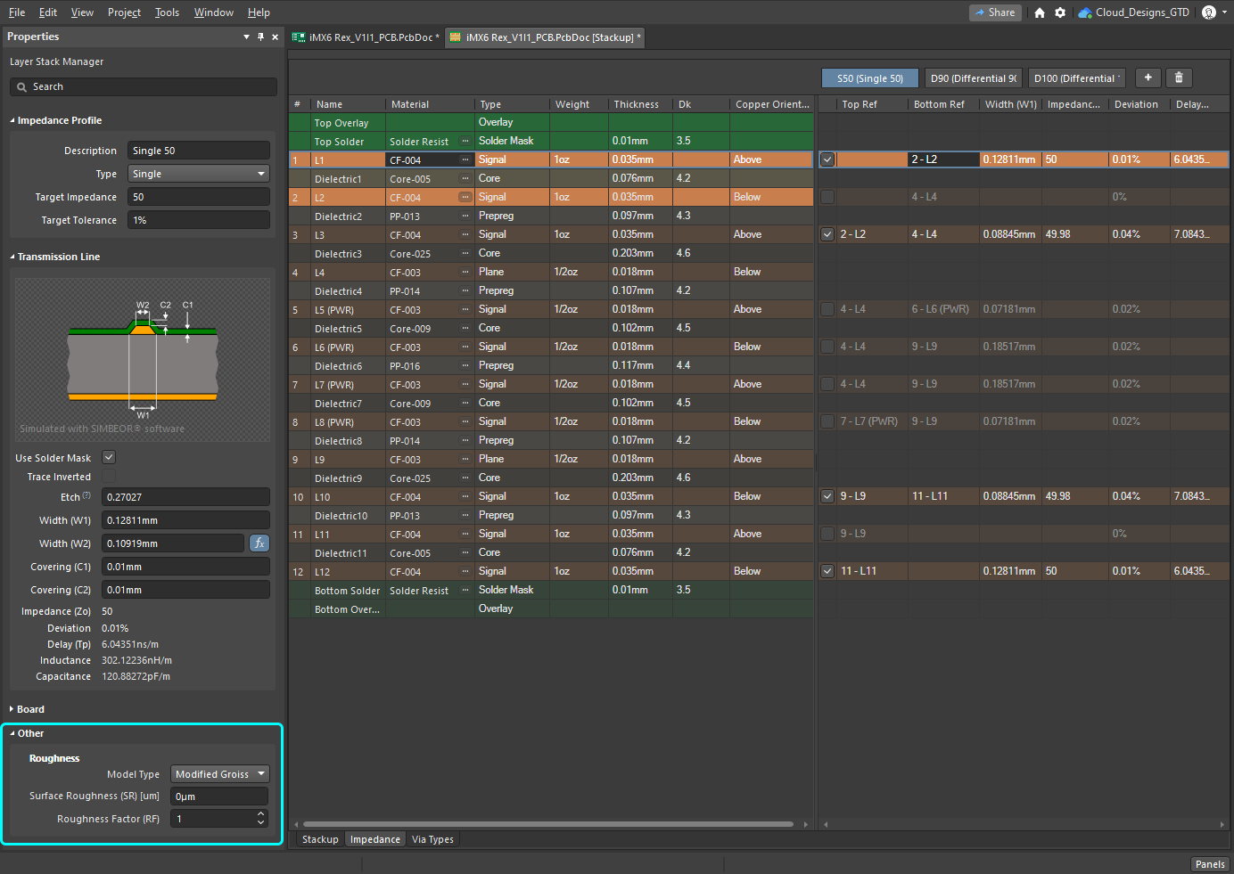 Surface roughness is included in the calculation of the characteristic impedance.
Roughness:
- Model Type - preferred model for calculating the impact of surface roughness (refer to the articles below for more information on the various models). Applies to all copper layers in the substack.
- Surface Roughness - value of the surface roughness (available from your fabricator). Enter a value between 0 to 10µm, default is 0.1µm
- Roughness Factor - characterizes the expected maximal increase in conductor losses due to the roughness effect. Enter a value between 1 to 100, default is 2.
Further reading
- Practical methodology for analyzing the effect of conductor roughness on signal losses and dispersion in interconnects: Y. Shlepnev, C. Nwachukwu, DesignCon2012.
- Unified approach to interconnect conductor surface roughness modelling: Y. Shlepnev, 2017 IEEE 26st Conference on Electrical Performance of Electronic Packaging and Systems (EPEPS2017)
Support for Coplanar Transmission Line Structures
The impedance calculator in the Layer Stack Manager supports single and differential coplanar structures. Create a new impedance profile, then select Single-Coplanar or Differential-Coplanar from the Impedance Profile Type drop-down list.
Working with coplanar structures:
- As with the standard single and differential impedances, values for each variable are automatically calculated based on the user-defined Target Impedance and Target Tolerance, and the physical properties of the board layers. These automatically calculated values can be adjusted by entering new values into the edit boxes of the Layer Stack Manager mode of the Properties panel.
- To target the signal nets you want to be routed with a coplanar structure, configure a Routing Width (or Differential Pairs Routing) design rule with the Use Impedance Profile option enabled, and the required Coplanar Impedance Profile selected.
- Coplanar structures require a reference plane on both sides of the signal route; this can be created by a polygon you place, or if stitching vias are added, by the Add Shielding to Net command (more info below). If you are placing a polygon, the separation between this polygon and the signal route is defined by the Clearance (S) value determined by Simbeor impedance calculator (displayed in the Properties panel, shown in the images above and below). Configure a Clearance design rule to control the clearance between the reference polygon and the signal route (show image).
- It is common practice to include a via fence along each side of the signal trace when the coplanar structure is grounded, use the Tools » Via Stitching/Shielding » Add Shielding to Net command in the PCB editor to do this. As well as placing vias, by enabling the Add shielding copper option this command can also place a polygon around the signal routing to cover the via fence, as shown in the image on the right, below.
► Learn more about Via Shielding
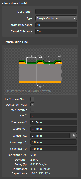
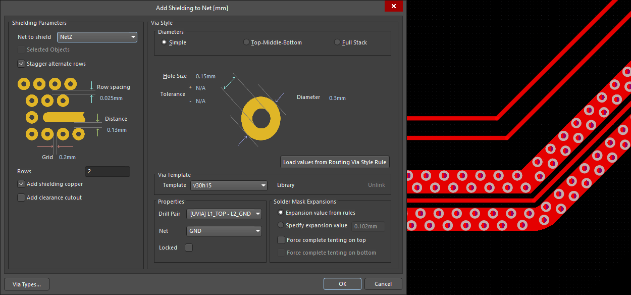 The impedance calculator determines the signal properties and clearances (first image), use that clearance in the via shielding Distance setting.
Selecting the Layer Material
In a controlled impedance design, the selection of the materials used in the layer stackup is very important.
For example, the most common material used to fabricate PCBs is glass fiber (fiberglass) reinforced epoxy resin, with copper foil bonded onto each side. The tightness of the weave of the glass fiber fabric affects the value and consistency of the dielectric constant Dk (permittivity) and Loss Tangent Df. Surrounding the woven glass fabric is resin - the percentage of resin used is also important in the performance of the material.
There is a large range of glass fiber weaves available. To help ensure the predictability and performance of the glass fiber-based materials used in PCB fabrication, the IPC have a standard for weaves:
IPC standard IPC-4412B: Specification for Finished Fabric Woven from "E" Glass for Printed Boards
The Material Library
As the designer, you can either edit the material properties directly in the Layer Stack Manager, or select materials from the Altium Material Library.
The entire library can be viewed (and added to) in the Altium Material Library dialog (Tools » Material Library).
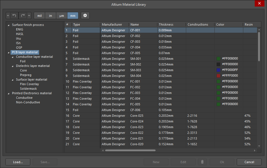
The materials are organized into usage categories, accessed through a tree structure on the left of the dialog. Below this level, each usage category is broken into functional categories, such as: Conductive layer material, Dielectric layer material and Surface Layer Material; in the PCB layer material category.
Adding, Saving and Loading Material
New material can added to the library when a specific material category is selected in the tree. Materials defined in an external material library can be loaded (Load button), and user-defined material that has been added in the Altium Material Library dialog can also be saved to a user-library (Save button). Only user-defined material is saved.
Adding Custom Properties to Material
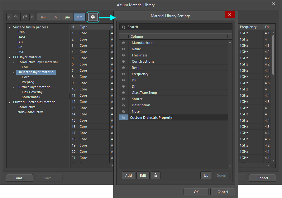
Custom properties can be added to material detailed in the library (default and user-defined material). To add a custom property, first select the correct node in the tree on the left to define the material(s) it is to be added to, then click the ![]() button to open the Material Library Settings dialog.
button to open the Material Library Settings dialog.
The required value can then be added to the selected material in the Altium Material Library dialog, select the row and click the Edit button.
Applying the Impedance Profile to the Routing
Controlled impedance routing is all about configuring the routing width to deliver the correct impedance, which means the routing width may be different on each signal layer. This is managed by assigning an Impedance Profile instead of a specific routing width when the design rule is configured in the PCB Rules and Constraints Editor (Design » Rules). When this is done the software automatically sets the width to suit the layer.
The required Impedance Profile is selected in the applicable Routing Width design rule (for individual nets), or Differential Pairs Routing design rule.
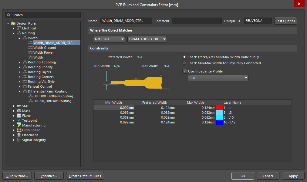 This routing width rule targets a class of DRAM nets. The S50 Impedance Profile is defining the routing widths, which will change according to the layer being routed on.
- Enable the Use Impedance Profile option in the Constraints region of the design rule. The dropdown list will include all available Impedance Profiles of the appropriate Type (Single or Differential), select the profile required by the nets being targeted by this design rule.
- When a profile is selected, that profile's Width settings are applied to the Preferred Width setting in the rule. This is done for each signal layer enabled for the profile, all other signal layers that are not enabled for that profile, are removed.
- When an Impedance Profile has been applied, the Preferred Width settings can no longer be edited. The Min Width and Max Width settings can still be edited, set these to suitable smaller/larger values.
- The nets can then be interactively routed, in the usual way.
► Learn more about Controlled Impedance Routing

