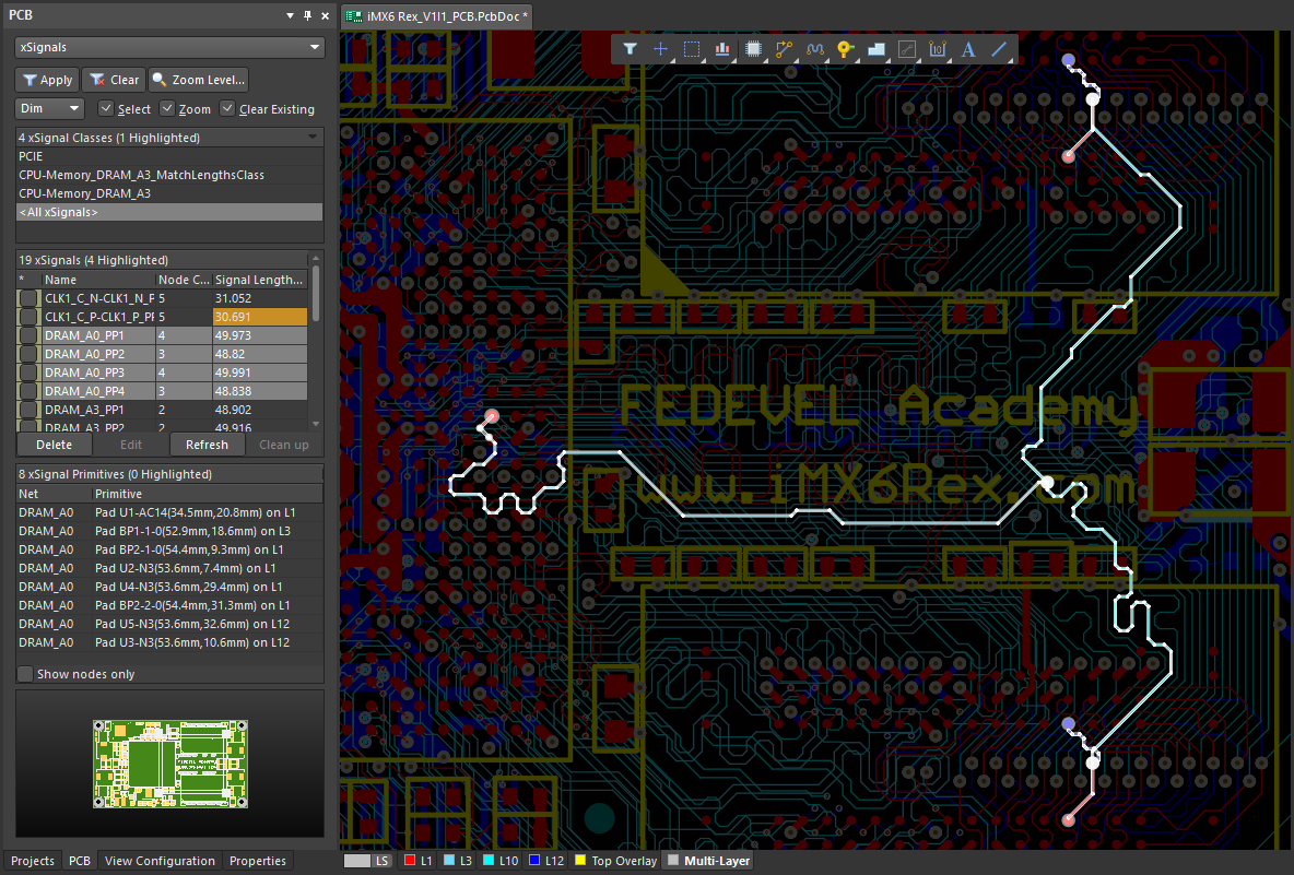
Defining High Speed Signal Paths with xSignals
The Challenge
With ever-increasing device switching speeds comes the challenge of maintaining the integrity of the signal, and meeting the signal's timing requirements. The signal integrity can be managed through controlled impedance routing, which is achieved through the careful design of both the PCB stackup and the routing widths to be used on each layer.
The timing requirements are met by matching the routed lengths of the signal paths. For a set of 2-pin signal paths, each running from an output pin to a single input pin, calculating and comparing the lengths is a straightforward process. This is not the case for many typical design solutions though where there may be a series termination component in the signal path, or there are more than two pins in the signal, which could then be routed using a Balanced T or a Fly-By routing topology, as shown in the image below.

Four DDR2 RAM chips routed using a Balanced T topology. ##
The Solution
The designer's job is to translate their design requirements, such as the maximum route length allowed to meet the timing budget, into a set of design rules, such as a Length rule to ensure that the timing is met, and a Matched Length rule to detect potential timing mismatches.
Now the designer sees the signals in terms of their function (eg, 'This address signal must be routed from this connector to each memory device. To achieve that I'll route using a fly-by topology with a termination resistor at the end. I might also require a series terminator at the source'). Even though address A0 passes through a termination resistor, to the designer, that signal is still A0 on the other side of that resistor.
But the PCB editor sees each signal simply as a set of connected pins (commonly referred to as a net) — Net A0 goes from this connector pin to this memory component pin, then to this memory component pin, and so on. As soon as a series termination resistor is added, that address line becomes two discrete nets. This makes it difficult for the designer to specify key design requirements, such as Length and Matched Length design rules.
This can be managed by a feature called xSignals (or extended Signal). This feature enables the correct treatment of a high-speed signal path as just that - a path for a signal to travel between a source and destination, through termination components as well as branches.
xSignal Query Keywords
The PCB editor includes a powerful and sophisticated filtering engine. This engine is used to identify objects when searching for objects in the design space, applying rules during interactive and automatic design tasks, and for checking rule compliance. The designer tells the filtering engine which objects they are interested in by writing a query, using query keywords recognized by the filtering engine.
The following xSignal type query keywords have been added for use in design rules and design space filters:
Membership Check Type Keywords
- InxSignal - Is the object in the specified xSignal, e.g.,
InxSignal('DRAM_A0_PP1') - InxSignalClass - Is the object in the specified xSignal class, e.g.,
InxSignalClass('PCIE') - IsxSignal - Is the object an xSignal with the specified name, e.g.,
IsxSignal('DRAM_A0_PP1')
Attribute Check Type Keyword
InAnyxSignal - Is the object in any xSignal, e.g., InAnyxSignal
Net-related Terminology
In the PCB editor, the following terminology is used:
- Net – a collection of components pins (nodes) that are connected to each other. The arrangement of how those nodes connect to each other is referred to as the topology; the default topology is shortest.
- From-To – conceptually, a From-To runs between two nodes in a net. The From-Tos can be created to follow the topology or arrangement of nodes in that net. For example, the net topology could be from R1-1 to U1-5 to U3-2 to R5-2. This net could have three From-Tos: R1-1 to U1-5; U1-5 to U3-2; and U3-2 to R5-2. If the topology is changed so will the possible From-Tos. From-Tos are created in the From-To mode of the PCB panel by either clicking the Generate button to create them based on a topology, or by selecting two pads in a net then clicking the Add From To button.
- xSignal – a user-defined set of nodes, typically a sub-set of a net (from this node to that node), or a combination of two nets that include a series component, such as a termination resistor.
