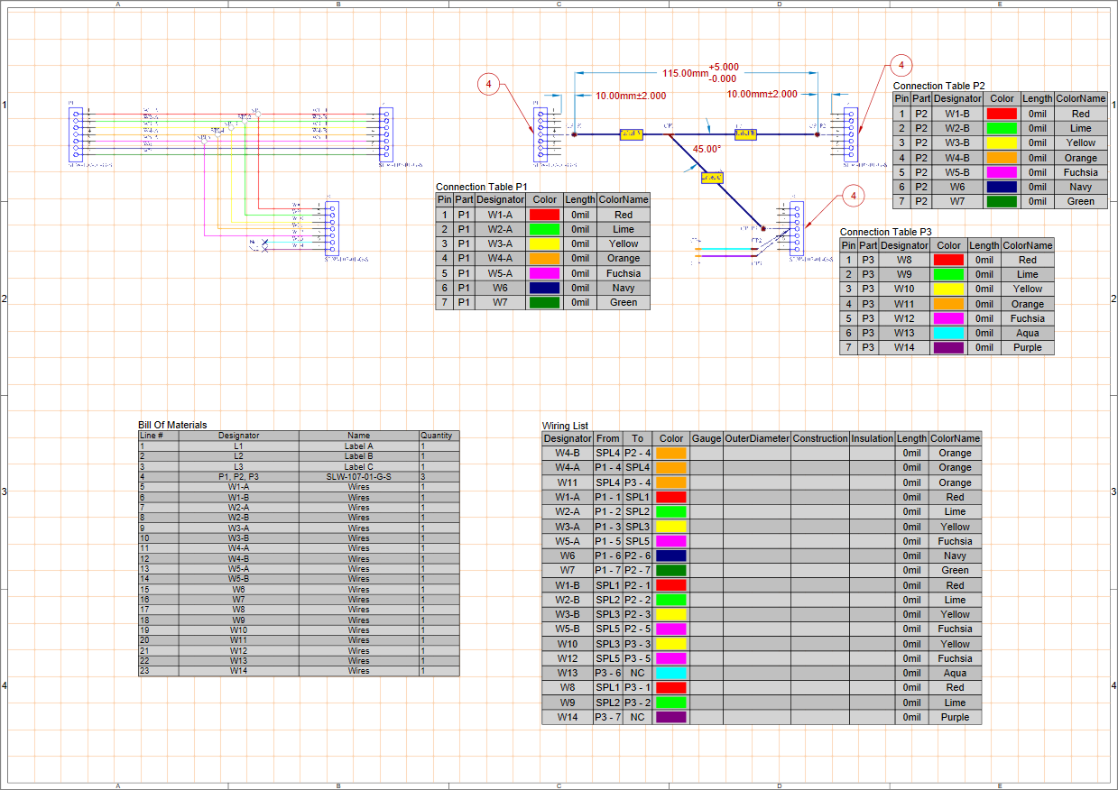
The Harness Design functionality allows engineers of various types (involved in the Product Design process) to work in Altium Designer. It brings comprehensive harness design support into the same environment as PCB and system design, removing the previous heavy reliance on third-party software.
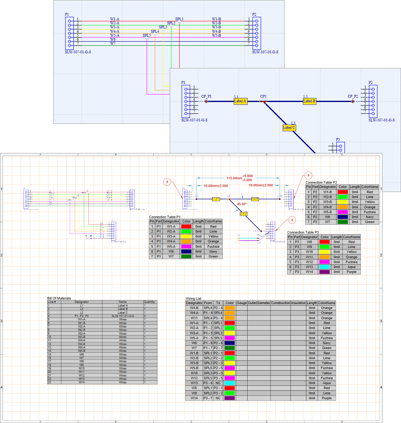
The Harness Design functionality allows you to create a full wiring harness design, from the individual pin-to-pin connections right through to manufacturing documentation. A harness design can be created as a standalone project, or as part of a Multi-board project. In the latter case, the logical connections between PCBs in the Multi-board project are used to define the connectivity within the harness.
The Harness Design functionality is available in both Altium Designer SE and full-featured Altium Designer.
Structure of a Harness Design Project
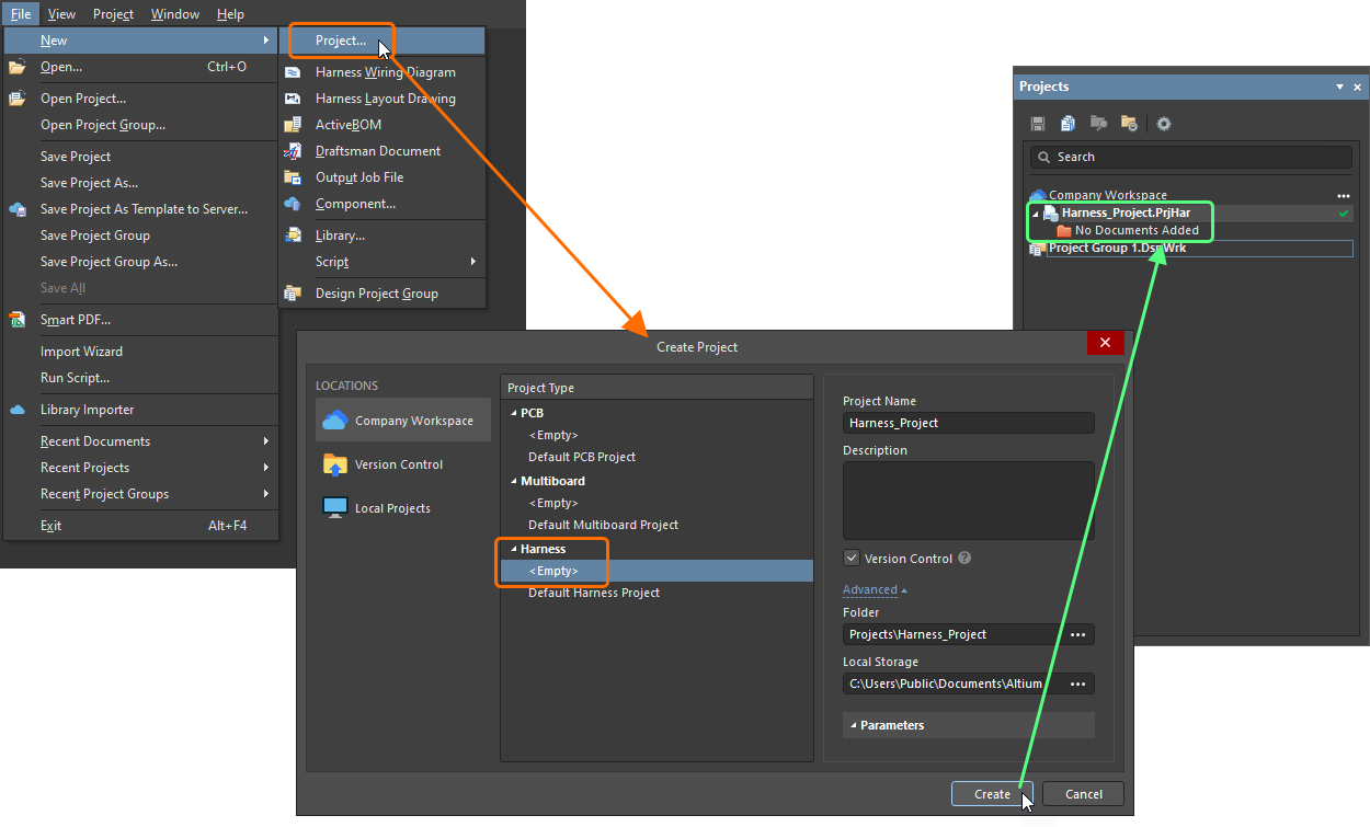
A new harness design project (*.PrjHar) can be created in the same way as a PCB or Multi-board design project. Select the File » New » Project command from the main menus to open the Create Project dialog. Select the <Empty> entry or an available project template in the Harness list.
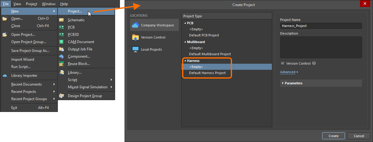
A harness design project supports the following documents:
- Harness Wiring Diagram (
*.WirDoc) – individual wires and cables are placed to create the required physical connections within the harness.
- Harness Layout Drawing (
*.LdrDoc) – the wires and cables are arranged to represent the physical construction of the harness.
- ActiveBOM (
*.BomDoc) – contains the following entities:
- Connectors and their associated parts
- Associated parts of splices
- Associated parts of connection points
- Cavities
- Layout labels
- Harness coverings
- Wire and cables, as well as their length values
For
harness wiring components, the
Length column in the ActiveBOM document presents the total length for wires/cables of the same BOM item rather than their individual lengths –
![]() show image
show image.
The source for BOM data of a harness design project is the project's Layout Drawing. So if the Wiring Diagram of your harness design was changed and this change should be reflected in the BOM, the Layout Drawing must be updated first.
- Draftsman Document (
*.HarDwf) – read-only views of the wiring diagram, layout drawing and BOM are imported, and any additional information required for the manufacturing of the harness is added.
-
Output Job File (*.OutJob) – a set of required outputs for your harness design can be pre-configured using an Output Job file. Each output is configured with its own settings and its own output format, for example, output to a file or to a printer. The same Output Job file configured for a harness design project can then be reused between designs, saving time and effort in preparing outputs for each new design.
While Output Job files facilitate streamlined preparation and generation of outputs, your harness design outputs can also be generated directly from the project documents (e.g., using the File » Print command for a Harness Wiring Diagram or Harness Layout Drawing document or Reports » Bill of Materials command for an ActiveBOM document).
Outputs Supported for a Harness DesignExpandCollapse
Documentation Outputs
- Harness Wiring Diagram Prints
- Harness Layout Drawing Prints
- Draftsman
Report Outputs
- Bill of Materials
- BOM Compare
- Export Comments
Validation Outputs
- BOM Checks
- Components states
- Configuration compliance
PostProcess Outputs
The set of Altium Designer's example projects includes a sample harness design project (Harness_Demo_Prj.PrjHar in the C:\Users\Public\Documents\Altium\AD<version>\Examples\Harness Demo MB\Harness_Demo_Prj folder by default), which is associated with a multi-board demo project (\Examples\Harness Demo MB\Harness_Demo_MB\Harness_Demo_MB.PrjMbd), so you can take harnesses for a test drive straight out of the box.
Adding a Harness Design Project to a Multi-board Project
A harness design project can (but does not need to be) be included as part of a Multi-board project. To do this, open a Multi-board project with a schematic document that contains at least one harness connection object. Ensure that the harness definition has been completed: harness connector parts assigned, harness connector ↔ PCB pin connections specified, and harness connector ↔ harness connector connections specified.
Add the harness project to the Multi-board project by right-clicking on the Multi-board project entry in the Projects panel and selecting Add Existing to Project and then browsing to and selecting the local .PrjHar file. The harness project will appear in the Projects panel within the Multi-board project structure.
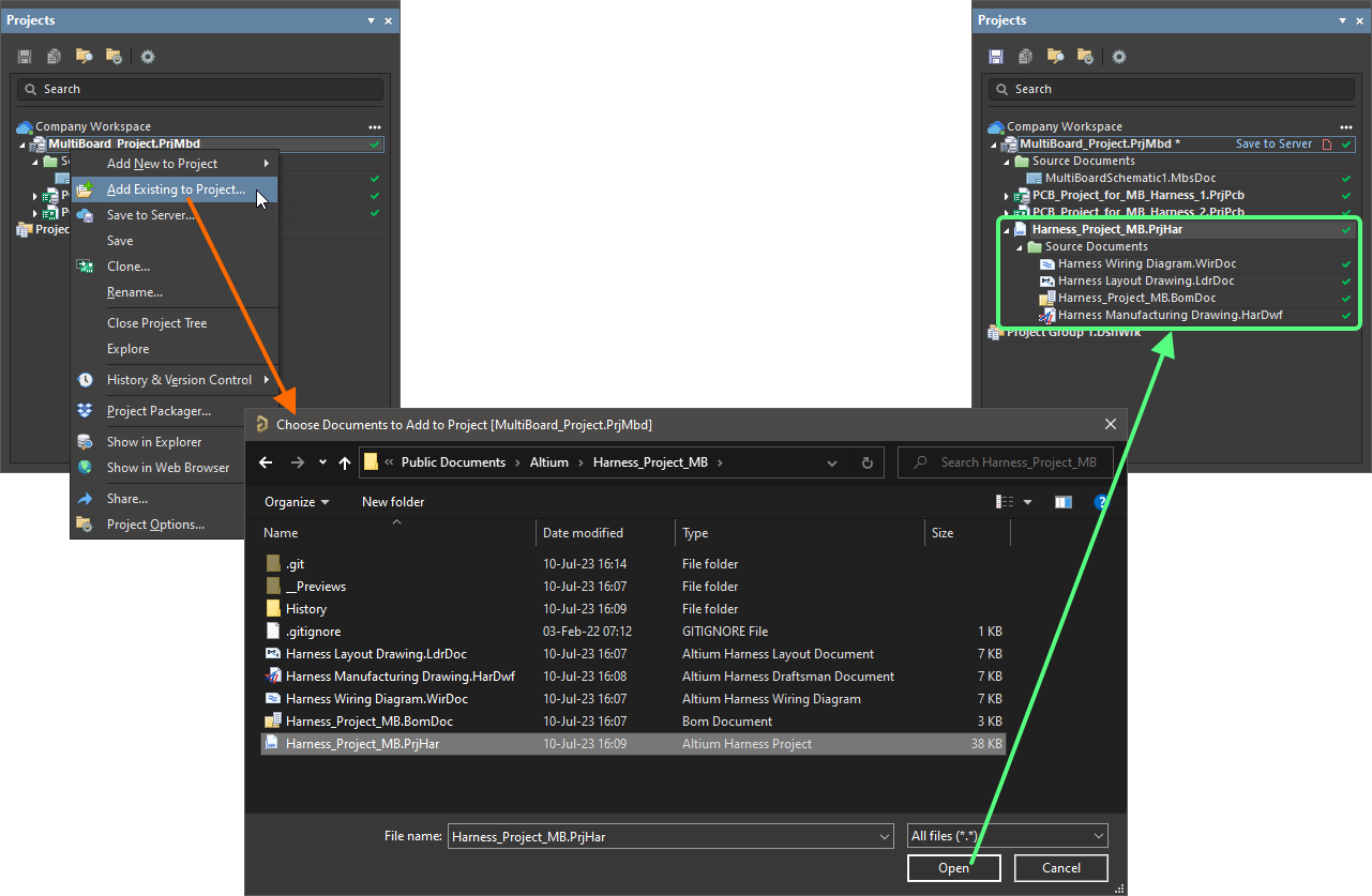
Add a created harness project to the related Multi-board project.
To add an existing harness project saved to a Workspace to a Multi-board project, open this harness project from the Workspace first (File » Open Project) to create its local working copy and then add it to the Multi-board project as described above.
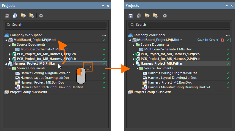
If a Harness Design project is already open, it can be added to the Multi-board project using the drag-and-drop action. Drag the entry of the harness project to the Multi-board project structure in the Project panel to include the harness design in this Multi-board project.
Creating a Harness Design – Example Guide
The collapsible sections below provide step-by-step instructions that will allow you to create a simple three-component harness design from scratch.
Creating a Harness Design ProjectExpandCollapse
- Select the File » New » Project command from the main menus.
-
The Create Project dialog will open:
- In the Locations list, select the entry for your Workspace (or the Local Projects entry if you are not using a Workspace).
- In the Project Type list, choose the <Empty> entry under the Harness type.
- Enter a suitable name in the Project Name field, e.g.,
Harness_Project.
- Set other options on the right-hand side of the dialog as required (e.g., the storage folder) and click the Create button.
- A new project will be created, and the project entry will appear in the Projects panel.
Defining the Wiring DiagramExpandCollapse
-
Right-click the harness project entry in the Projects panel and select the Add New to Project » Harness Wiring Diagram command from the context menu.
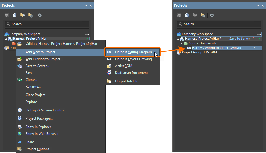
- A blank sheet of a new Harness Wiring Diagram document will appear. Save it on your hard drive by right-clicking its entry in the Projects panel and selecting the Save As command from the context menu. The Save As dialog will open, ready to save the document in the same location as the project file. Type
Harness Wiring Diagram in the File name field and click Save (there is no need to type in the extension, as it will be added automatically).
- Since you added a new document to the project, the project file has changed. Right-click on the project entry in the Projects panel, then select the Save command from the context menu to save the project structure changes.
-
Place connector components on the wiring diagram. Normally, you would use components from your own libraries accessed from the Components panel. In this example, manufacturer parts will be used directly:
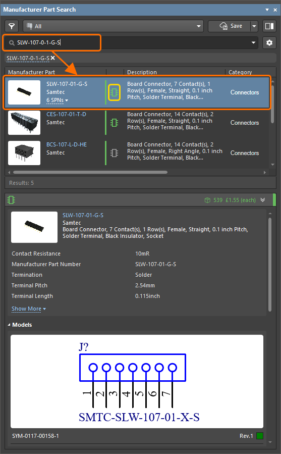
- Open the Manufacturer Part Search panel (to open a panel, click the Panels button at the bottom-right of the design space and select the required entry from the menu that opens).
-
In the Search field of the panel, enter SLW-107-0-1-G-S and press Enter. Found components will be shown in the search results region of the panel. For this example, a component with a schematic symbol model is needed. Components with models are indicated with the  icon in the list.
-
Select a suitable component, right-click it, and select the Place command from the context menu. The cursor will change to a crosshair, and the component symbol will be floating on your cursor in the wiring diagram design space. You are now in component placement mode. If you move the cursor around, the component will move with it.
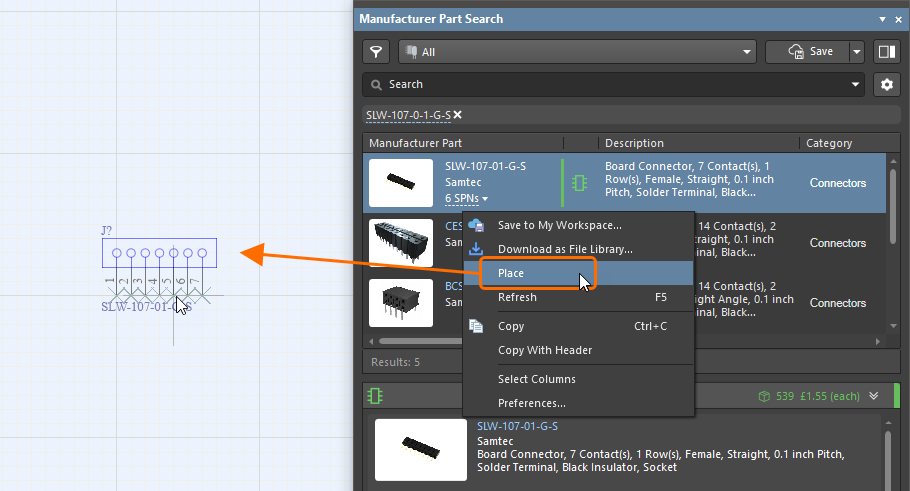
- While the component is still floating on the cursor, press the Tab key to open the Properties panel to edit component properties.
-
In the Properties region of the panel, type in the Designator P1.
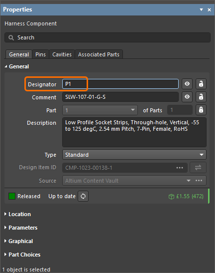
- Leave all other fields at their default values, then click the pause button in the design space (
 ) to return to component placement.
- Use the Spacebar to rotate the component by 90 degrees and the X and Y keys to flip it horizontally and vertically, respectively.
- Once you are happy with the component's location and orientation, click the left mouse button to place the component onto the document. The location can be changed later if required.
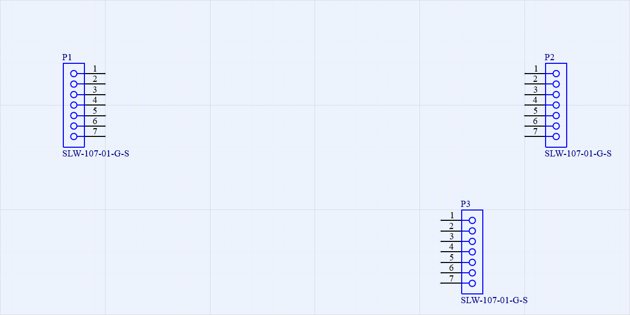
- Move the cursor, and you will find that a copy of the connector has been placed on the wiring diagram, and you are still in part placement mode with the component symbol floating on the cursor. This feature allows you to place multiple components of the same type. The designators of subsequentially placed components (during a single placement session) will be incremented automatically.
- Place the second and third connectors according to the images below.
- Since all connectors have been placed, exit part placement mode by clicking the right mouse button or pressing the Esc key. The cursor will revert back to a standard arrow.
If you need to change a placed component's location or orientation, click and hold the left mouse button on it and drag the mouse to the required location. During the drag, use the Spacebar, X and Y key to rotate, flip horizontally and flip vertically, respectively.
-
Component pins are connected using physical wires:
- Select the Place » Harness Wire command from the main menus.
- Click the connection point of pin
P1-1 (a red cross appears at the cursor when it’s over a pin connection point) to place the start point of the wire, and then click the connection point of pin P2-1 to place the endpoint of the wire.
- Similarly, connect other pins of
P1 and P2 (P1-2 ↔ P2-2, P1-3 ↔ P2-3, etc.).
- Once the wires are placed, right-click to exit the command.
-
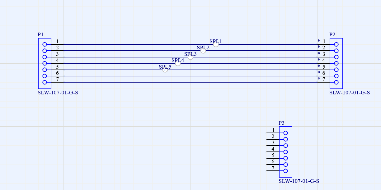
Additional wires should be connected to already placed wires. In such cases, a splice or tap should be placed first. Splices will be used in this example:
- Select the Place » Splice command from the main menus.
- Press the Tab key to open the Properties panel to edit splice properties.
- Type in
SPL1 in the Designator field of the Properties panel.
- Click the pause button in the design space (
 ) to return to splice placement.
- Place five splices on previously placed wires, as shown in the image below. Each wire will be split in two by the splice.
- Once the splices are placed, right-click to exit the command.
-
Place additional wires between the splices and pins of P3, as shown in the image below.
By default, a wire is placed in 90 degree placement mode. In this mode, press the Spacebar to change direction of the wires being placed if required.
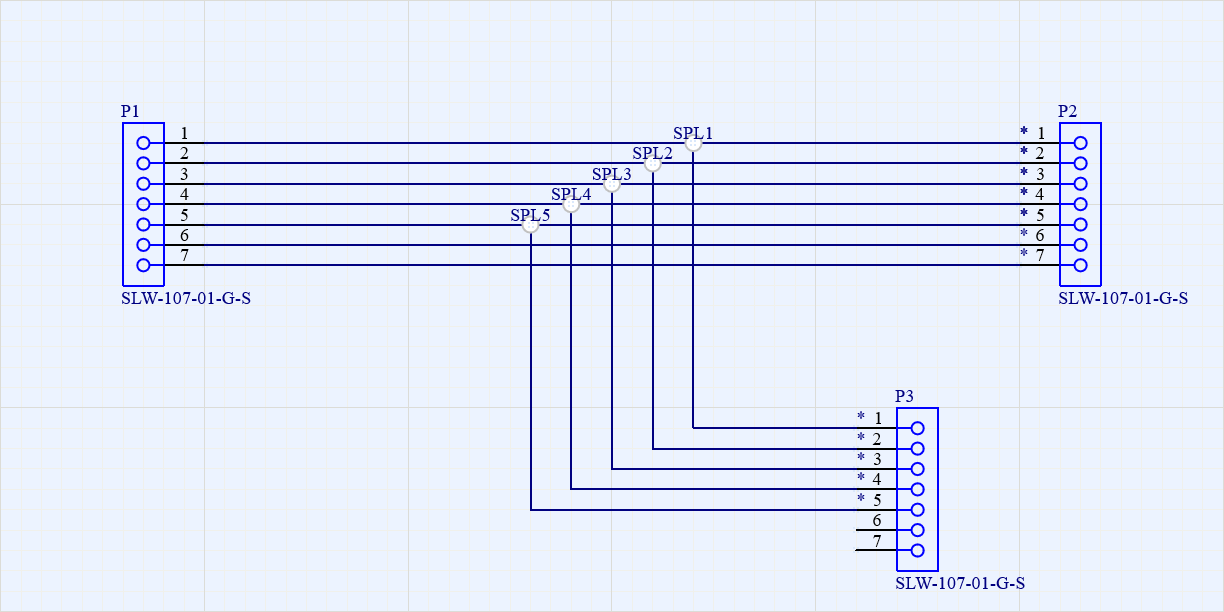
-
Place additional unconnected wires to pins P3-6 and P3-7 and mark them as unconnected:
- Select the Place » Harness Wire command from the main menus.
- Click the connection point of pin
P3-6 to place the start point of the wire, and then click a point in the design space away from other objects at the left of the pin to place the endpoint of the wire, as shown below.
- Right-click to finish placement of the wire. Note that the unconnected wire end is indicated with a solid square.
- Click the connection point of pin
P3-7 to place the start point of the wire, and then click a point in the design space away from other objects at the left of the pin to place the endpoint of the wire, as shown below.
- Right-click to finish placement of the wire.
- Since a wire should not be left unconnected, No Connect objects should be placed at the unconnected ends of wires. Select the Place » No Connect command from the main menus.
- During placement, press the Spacebar to set location of the No Connect object's name.
- Place a No Connect object (
Nc1 and Nc2) at each unconnected wire end.
-
Configure the display of placed wires, as shown in the image below. To edit a wire, double-click it in the design space to open the Properties panel, where you can:
-
Set the wire's Designator and enable its visibility by clicking the visibility icon at the right of the Designator field (the icon should be shown as  ).
).
To change location of a wire designator in the document, click and hold the left mouse button on it in the design space and drag it to the desired location.
- Disable visibility of the wire's Comment by clicking the visibility icon at the right of the Comment field (the icon should be shown as
 ).
).
- Choose the wire color by clicking the color swatch in the Value column for the Color parameter in the Parameters region.
- Save the changed Wiring Diagram document by right-clicking its entry in the Projects panel and selecting the Save command from the context menu.
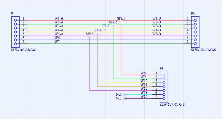
Creating the Layout DrawingExpandCollapse
-
Right-click the harness project entry in the Projects panel and select the Add New to Project » Harness Layout Drawing command from the context menu.
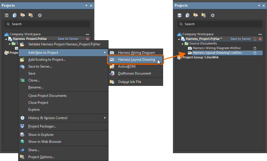
- A blank sheet of a new Harness Layout Drawing document will appear. Save it on your hard drive by right-clicking its entry in the Projects panel and selecting the Save As command from the context menu. The Save As dialog will open, ready to save the document in the same location as the project file. Type
Harness Layout Drawing in the File name field and click Save (there is no need to type in the extension, as it will be added automatically).
- Right-click on the project entry in the Projects panel, then select the Save command from the context menu to save the project structure changes.
-
Select the Design » Import Wiring Diagram command from the main menus to import the design data from the wiring diagram. The connectors will be inserted into the layout drawing sheet in the relative positions defined in the wiring diagram. Connection points associated with connectors will also be placed next to each connector on the layout drawing.
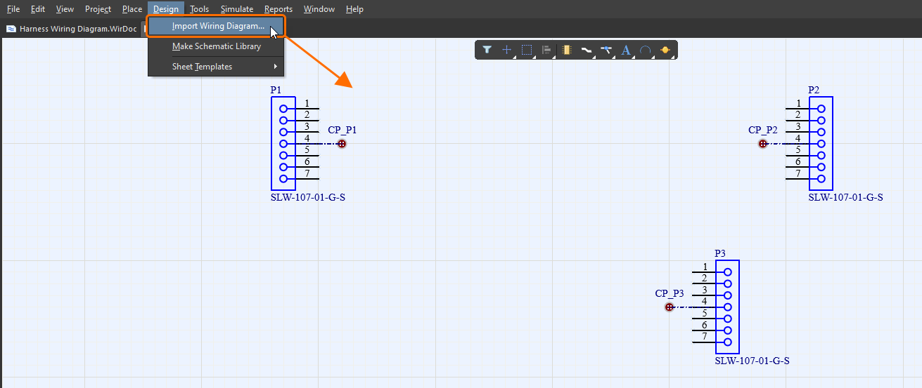
-
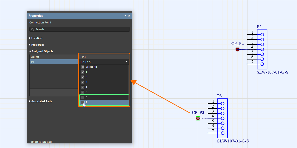
For the connection point associated with P3, only pins 1-5 should be selected. Select CP_P3 and deselect pins 6 and 7 in the Pins drop-down of the P3 entry in the Assigned Objects region of the Properties panel.
-
Physical connections are defined as harness bundles, each of which must start and end at a connection point. First, place a harness bundle starting at CP_P1 and ending at CP_P2.
- Select the Place » Harness Bundle command from the main menus.
- Click a connection point (a red cross appears at the cursor when it’s over a pin connection point) to place the start point of the harness bundle, and then click another connection point to place the endpoint of the harness bundle.
- Right-click to exit the command and confirm the placement of the harness bundle.
-
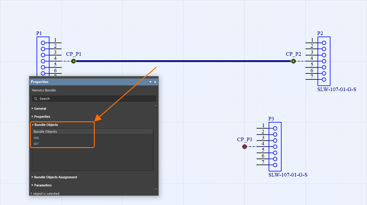
Select the placed bundle in the design space to see its properties in the Properties panel. The contents of the bundle can be seen in the Bundle Objects list. Note that the bundle includes wires W6 and W7 because these are the only two wires that directly connect P1 and P2.
-
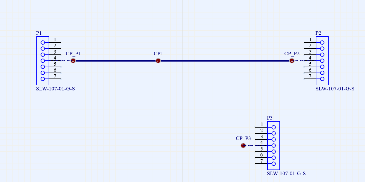
For the wires between pins 1-5 on P1 and P2 to be included in the bundle, the splices (that were placed in the wiring diagram) must be included in the layout drawing. Place a connection point (CP1) onto the bundle using the Place » Connection Point command from the main menus. This splits the original harness bundle into two separate bundles.
-
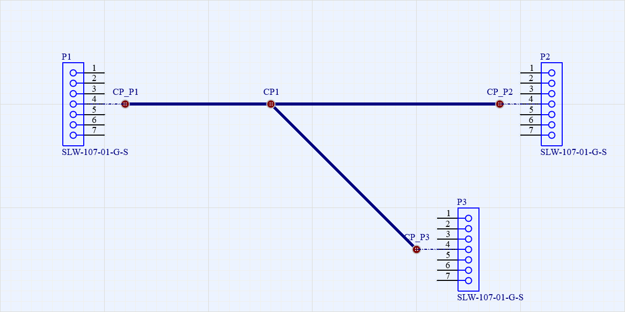
Place a harness bundle between connection points CP1 and CP_P3.
-
Select CP1 and confirm that each splice (SPL1, SPL2, SPL3, SPL4 and SPL5) is assigned to it.
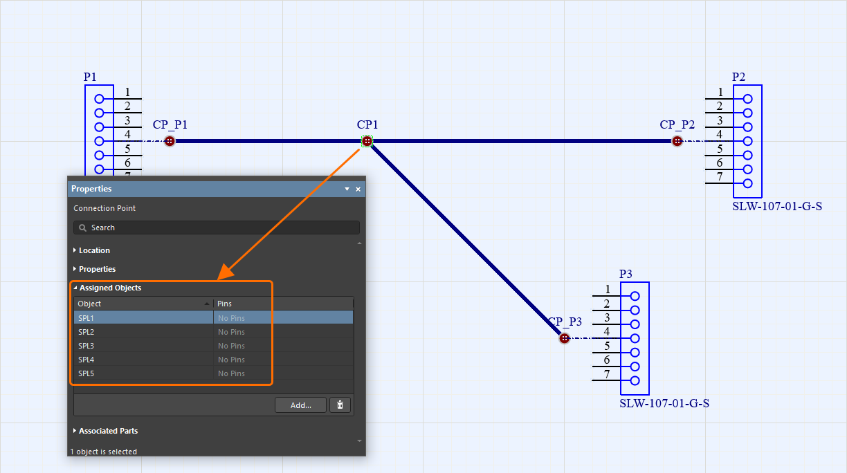
-
Each harness bundle will now automatically contain the correct wires. For example, select the harness bundle between CP_P1 and CP1 (the bundle attached to CP_P1/CP1) to see that it now contains W1-A, W2-A, W3-A, W4-A, W5-A, W6, and W7.
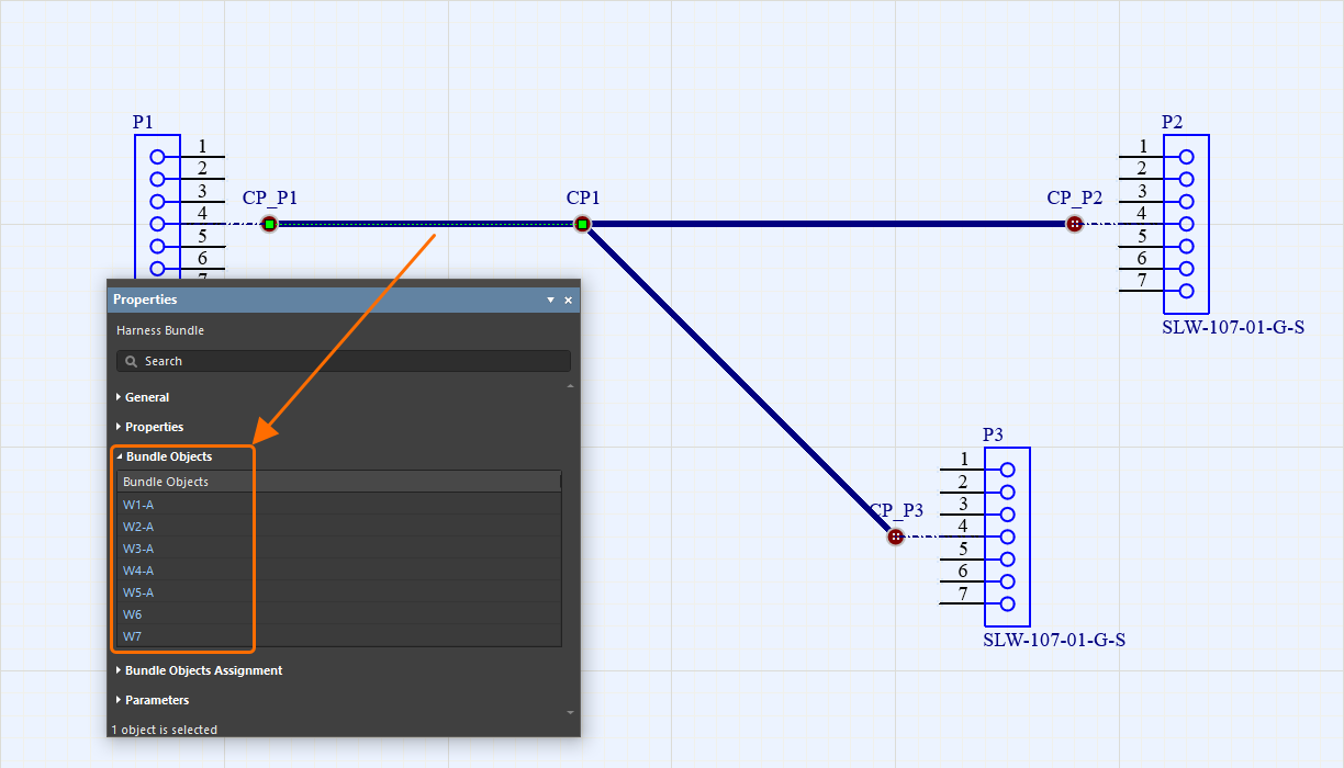
-
The symbol for a connection point can also be changed to improve its appearance. With the connection point CP1 selected, change its Style to Insulator in the Properties region of the Properties panel.
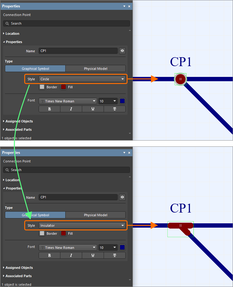
-
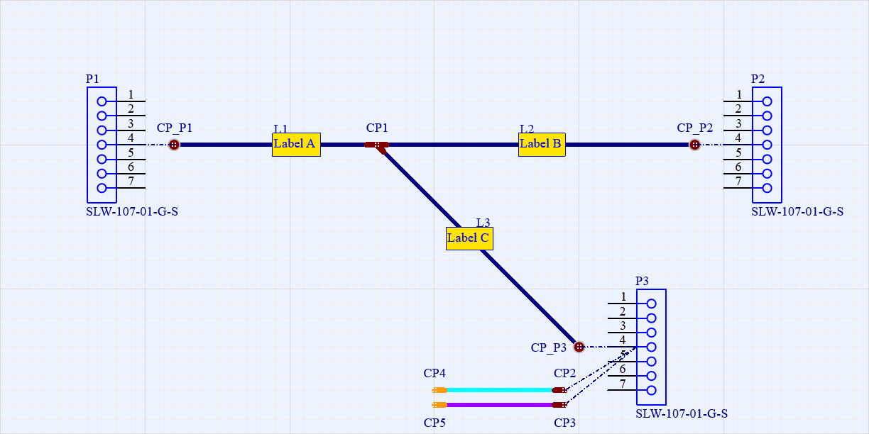
Individual wires can be represented in the layout drawing as bundles containing a single wire.
- Place two connection points (
CP2 and CP3) next to the connector P3.
- Select
CP2 and click the Add button in the Properties panel to open the Add Assigned Objects dialog. Select connector P3 in the dialog and click Add.
- Back to the Properties panel, select pin 6 of
P3.
- Select
CP3 and click the Add button in the Properties panel to open the Add Assigned Objects dialog. Select connector P3 in the dialog and click Add.
- Back to the Properties panel, select pin 7 of
P3.
- Place two more connection points (
CP4 and CP5).
- Select
CP4 and click the Add button in the Properties panel to open the Add Assigned Objects dialog. Select No Connect directive Nc1 in the dialog and click Add.
- Select
CP5 and click the Add button in the Properties panel to open the Add Assigned Objects dialog. Select No Connect directive Nc2 in the dialog and click Add.
- Place one bundle between
CP2 and CP4 and another between CP3 and CP5. The first bundle (CP2-CP4) will automatically contain W13 and the second (CP3-CP5) will contain W14.
- The appearance of the “wires” (bundles containing single wires) and the connection points associated with the unconnected ends can be changed to better represent their real appearance.
- Place physical labels using the Place » Layout Label command from the main menus. The properties of a label can be configured using the Properties panel when the label is selected in the design space. Place labels
L1, L2 and L3 on harness bundles and set text Label A, Label B and Label C for them, respectively.
- Save the changed Layout Drawing document by right-clicking its entry in the Projects panel and selecting the Save command from the context menu.
Validating the Harness DesignExpandCollapse
Before moving further, validate the harness design to make sure that the wiring diagram and layout drawing documents have no errors.
-
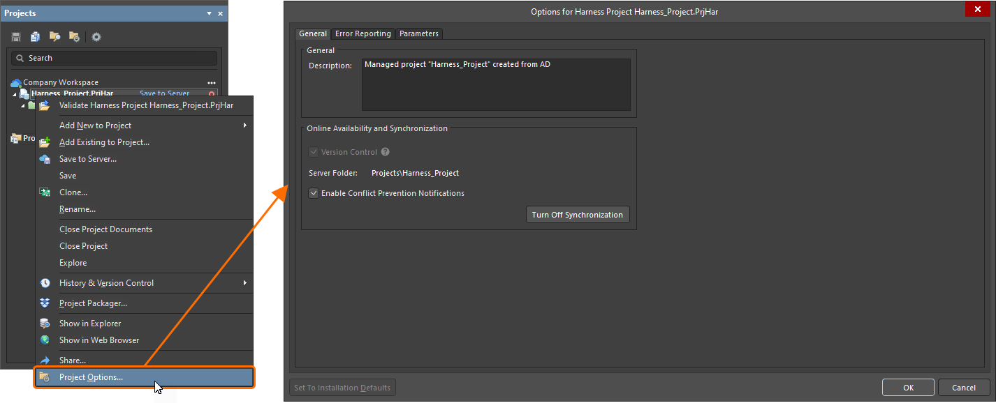
Right-click the harness project entry in the Projects panel and select the Project Options command from the context menu. The Project Options dialog will open.
-
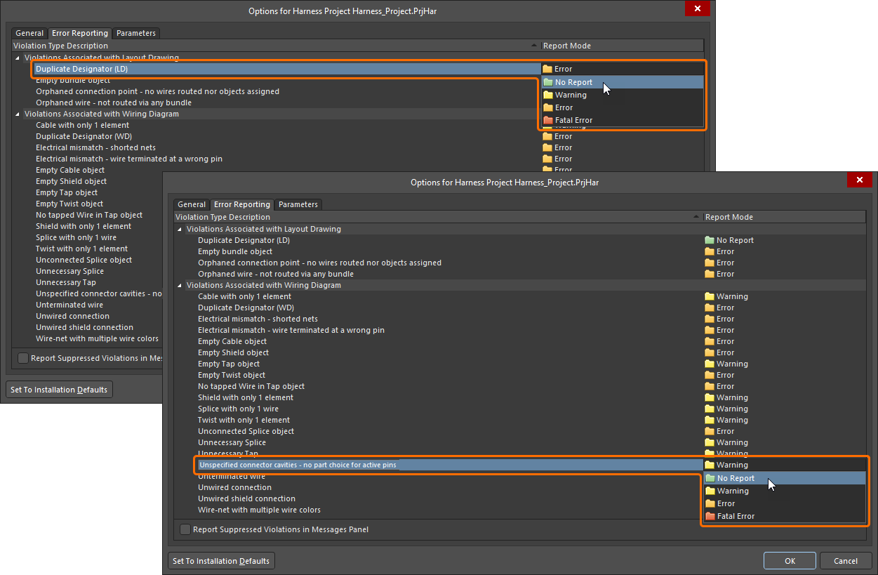
For this example design, disable some checks. On the Error Reporting tab of the Project Options dialog, click in the Report Mode column and select No Report for the following checks:
- Duplicate Designator (LD) (in the Violations Associated with Layout Drawing category)
- Unspecified connector cavities - no part choice for active pins (in the Violations Associated with Wiring Diagram category)
- Click OK in the Project Options dialog.
- Right-click on the project entry in the Projects panel, then select the Save command from the context menu to save the changes of project options.
-
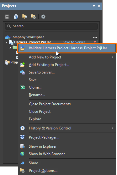
Right-click on the project entry in the Projects panel, then select the Validate Harness Project <ProjectName> command from the context menu.
-
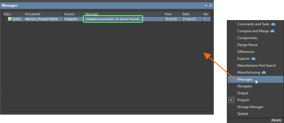
Open the Messages panel by clicking the Panels button at the bottom right of the design space and selecting Messages from the menu that appears. Make sure that the panel includes a single message: Compile successful, no errors found.
-
If there are warnings or errors listed in the Messages panel, resolve the violation conditions then perform validation again to make sure that the project contains no unresolved violations.
Double-click a violation message in the Messages panel to cross-probe to the offending object.
Creating the Manufacturing DrawingExpandCollapse
- Right-click the harness project entry in the Projects panel and select the Add New to Project » Draftsman Document command from the context menu.
-
In the New Document dialog that opens, select the [Default] template in the Templates list and confirm that the correct harness project is selected in the Project drop-down. Click OK in the dialog.
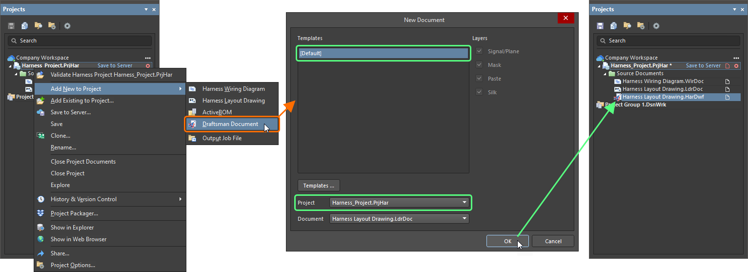
- The blank manufacturing drawing will be displayed. Save it on your hard drive by right-clicking its entry in the Projects panel and selecting the Save As command from the context menu. The Save As dialog will open, ready to save the document in the same location as the project file. Type
Harness Manufacturing Drawing in the File name field and click Save (there is no need to type in the extension, as it will be added automatically).
- Right-click on the project entry in the Projects panel, then select the Save command from the context menu to save the project structure changes.
-
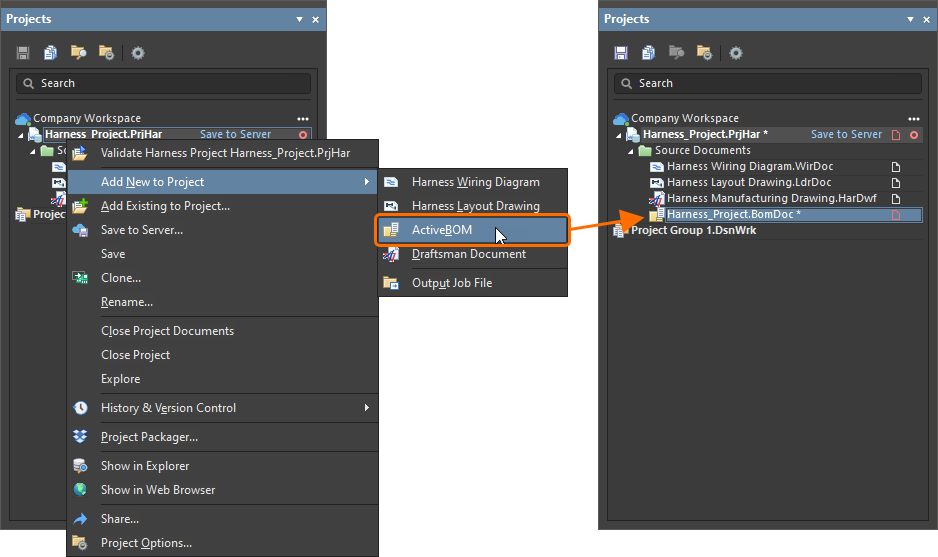
Before a drawing view can be placed, an ActiveBOM document must be added to the project. Right-click on the project entry in the Projects panel, then select Add New to Project » ActiveBOM command from the context menu.
-
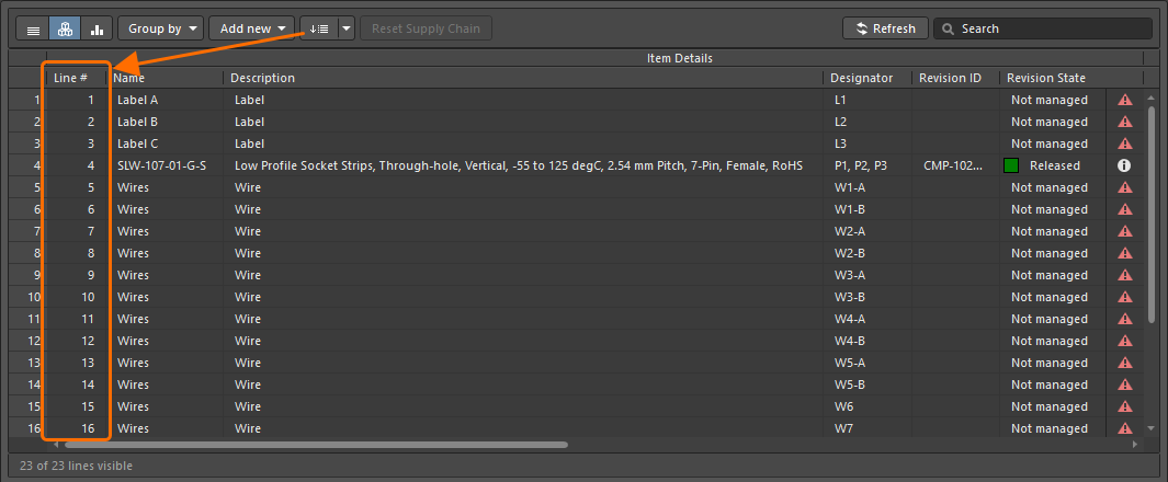
In the ActiveBOM document that opens, click the  button at the top of the document to set line numbers.
- Save the ActiveBOM document on your hard drive by right-clicking its entry in the Projects panel and selecting the Save As command from the context menu. The Save As dialog will open, ready to save the document in the same location as the project file. Leave the default name and location and click Save.
- Right-click on the project entry in the Projects panel, then select Save to save the project structure changes.
- Make the manufacturing drawing document the active document in the design space by clicking its document tab at the top of the design space.
-
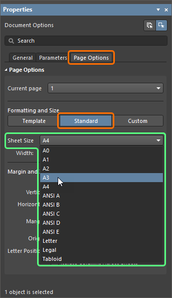
When there is no selected object in the design space, open the Properties panel, from where you can configure the document options. On the Page Options tab of the panel, select A3 from the Sheet Size drop-down when Standard mode is active for Formatting and Size.
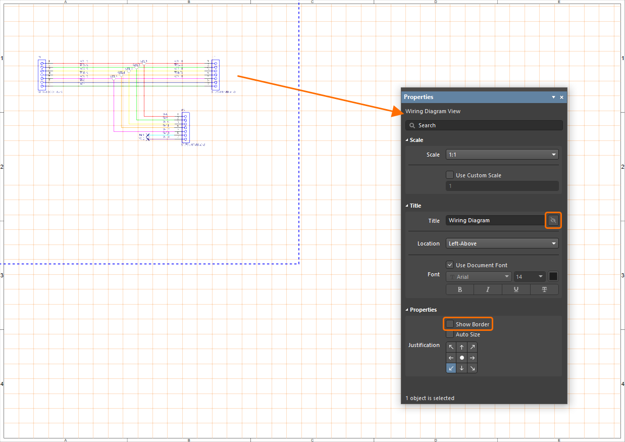
- Select the Place » Wiring Diagram View command from the main menus.
- The cursor will change to a crosshair, and the view will be floating on your cursor. Hover the cursor so the view is in the top-left part of the document sheet. Once you are happy with the view's location, click the left mouse button to place the view onto the document. The location can be changed later if required.
-
Select the Wiring Diagram View in the design space and disable visibility of the view's title and border in the Properties panel.
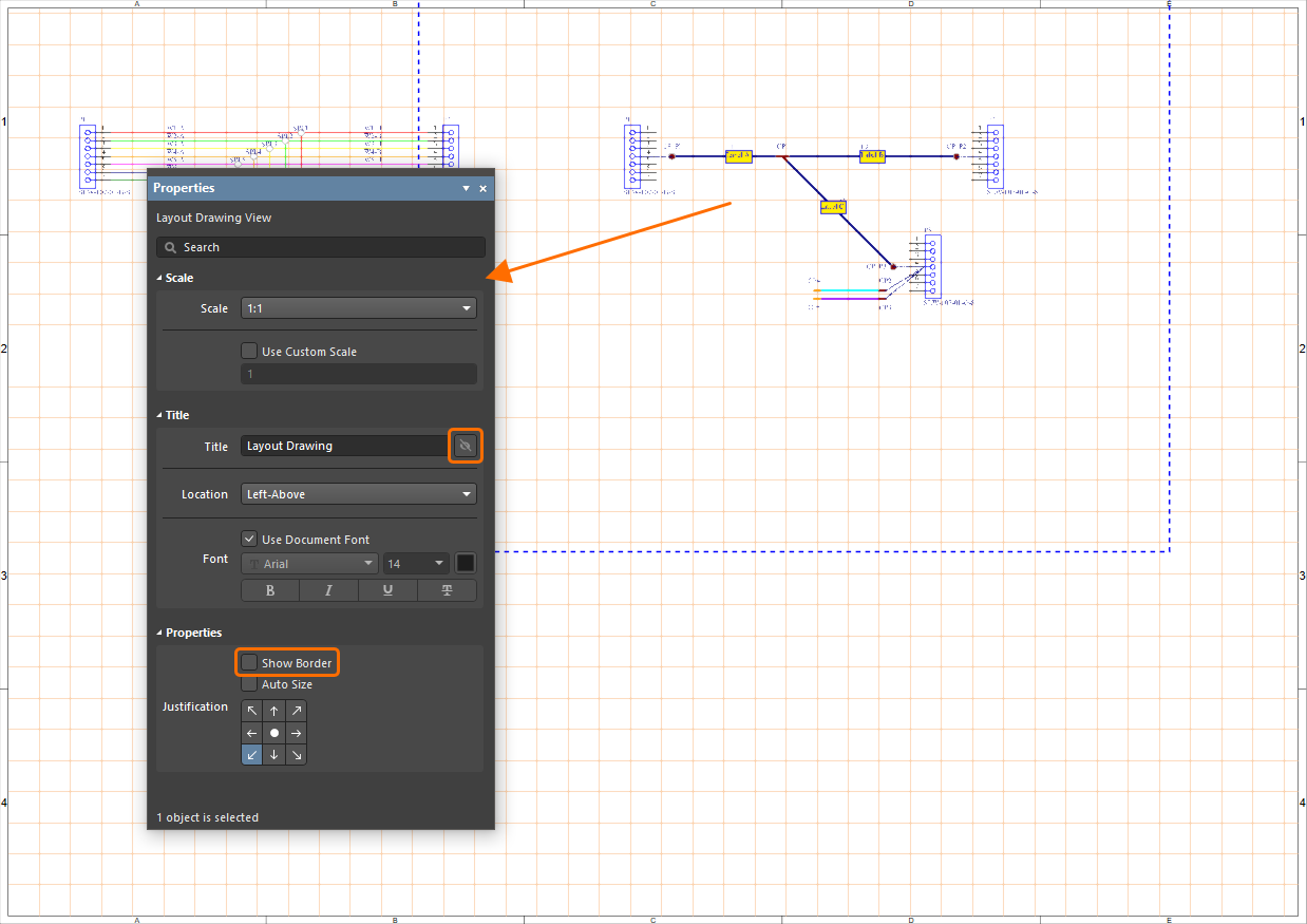
- Similarly, select the Place » Layout Drawing View command from the main menus and place the view in the top-right part of the document sheet.
-
Select the Layout Drawing View in the design space and disable visibility of the view's title and border in the Properties panel.
-
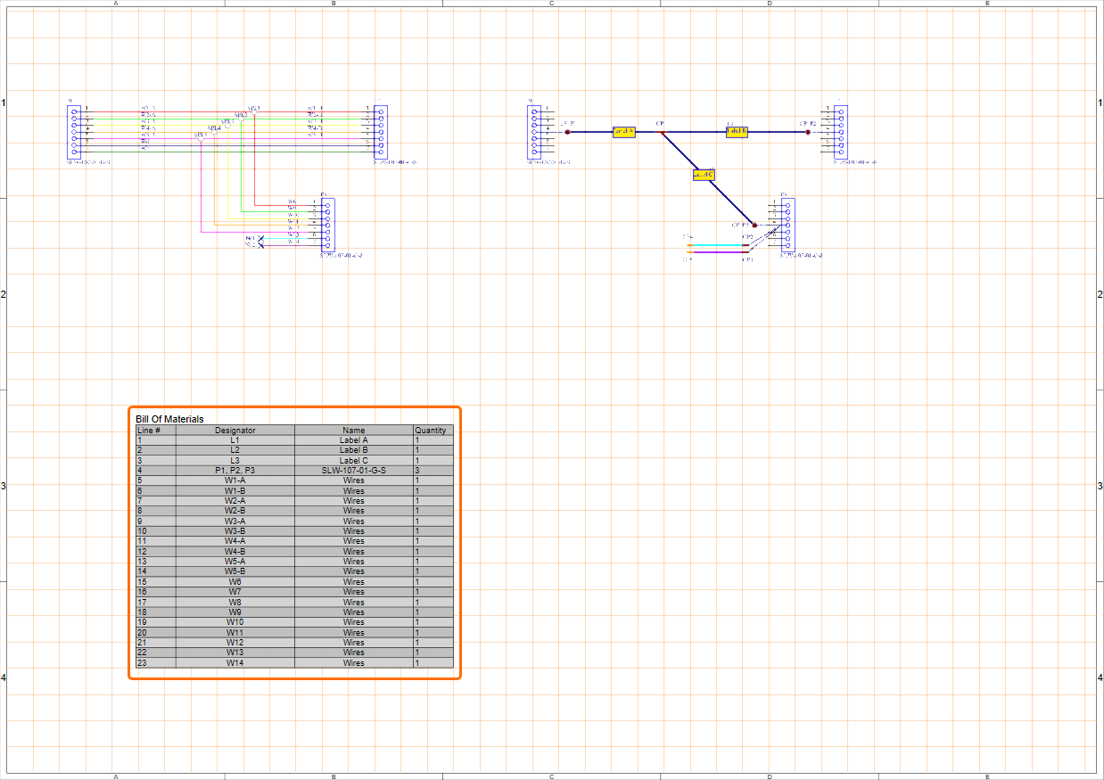
Select the Place » Bill of Materials command from the main menus and place the BOM table in a free space on the sheet.
-
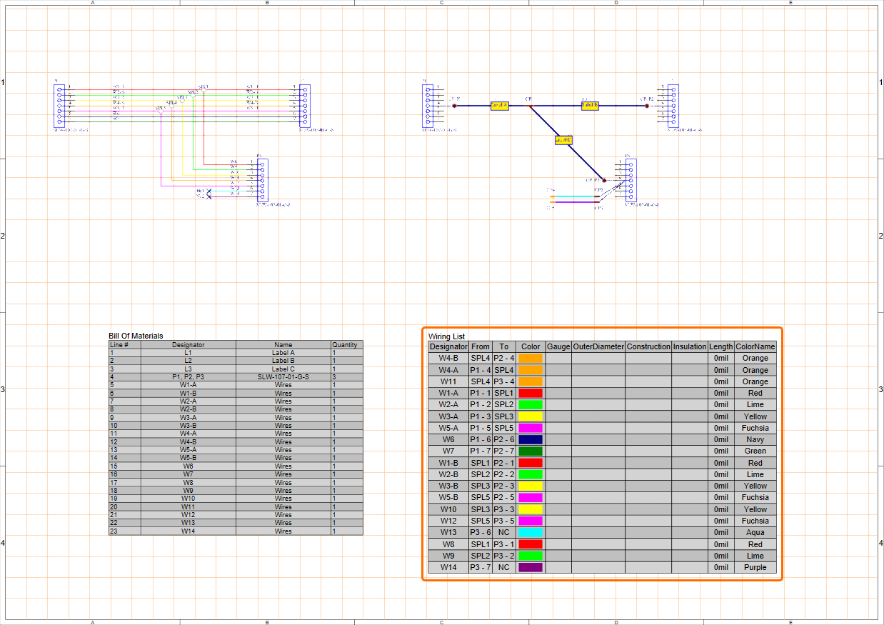
Select the Place » Wiring List command from the main menus and place the wiring list table in a free space on the sheet.
-
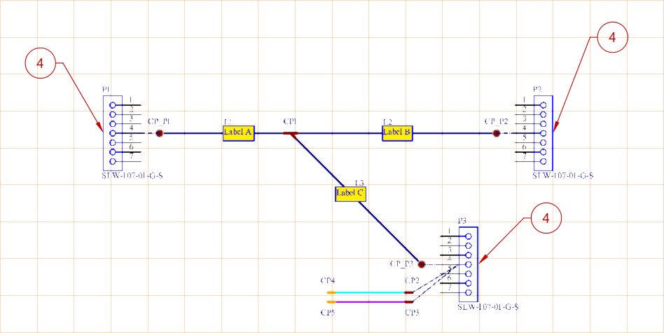
Callouts reflecting BOM item numbers can be placed in the manufacturing drawing:
- Select the Place » Annotations » Callout command from the main menus.
- Hover the cursor over a connector on the Layout Drawing View so an edge or a point of this connector is highlighted orange.
- Click to define location of the callout pointer.
- Move the cursor away from the connector and click to place the callout source text (BOM item number by default).
- Right-click to finish placement of the callout.
- You will remain in callout placement mode. Repeat the steps from
b to e to place callouts for the two remaining connectors.
- Right-click to exit callout placement mode.
-
Place a connection table for each connector:
- Select the Place » Connection Table command from the main menus.
- Place the table next to a connector on the Layout Drawing View.
- Select the connection table in the design space and open the Properties panel if not already.
- In the Component drop-down on the General tab of the panel, select the connector next to which the table is placed.
- If required, correct location of the table and/or the view by holding the left mouse button and dragging it to the required location.
- Repeat the steps from
a to e to place connection tables for the two remaining connectors.
-
Place dimensions on the Layout Drawing View according to the image below.
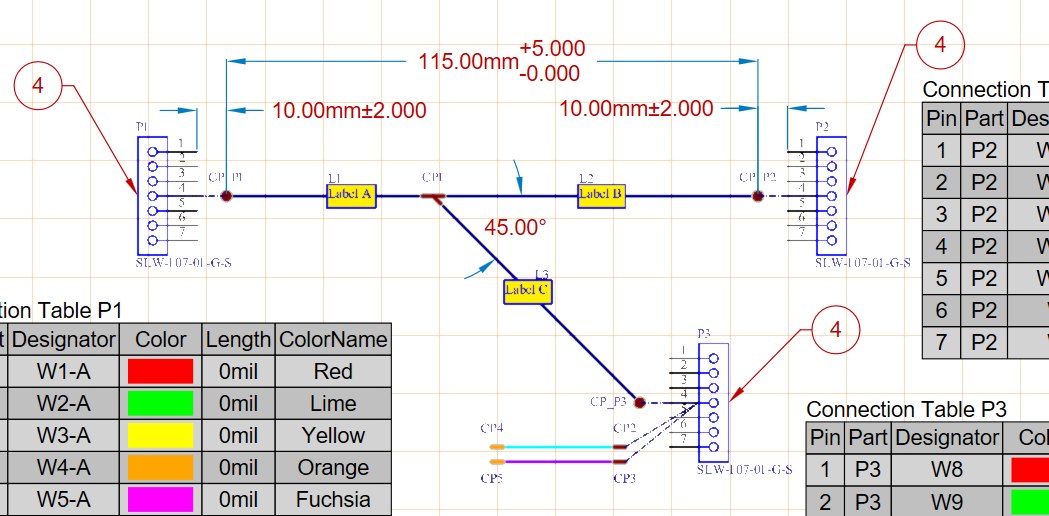
- To place a linear dimension, select the Place » Linear Dimension command from the main menus. Click once to define the first reference point, again to define the second reference point, and a third time to place the dimension text and its associated extension lines. Place another linear dimension or right-click to exit dimension placement mode.
- To place an angular dimension, select the Place » Angular Dimension command from the main menus. Click once to define the first reference line, again to define the second reference line, and a third time to set the position of the dimension text and the style of the angular dimension lines. Place another angular dimension or right-click to exit dimension placement mode.
- Various properties of a placed dimension can be modified in the Properties panel when the dimension is selected in the design space, including font, text/arrow configuration, value (manual override), and tolerances.
- Save the changed Manufacturing Drawing document by right-clicking its entry in the Projects panel and selecting the Save command from the context menu.
- If you created the harness design project in your connected Workspace, right-click the project entry in the Projects panel and select the Save to Server command from the context menu and click OK in the Save to Server dialog that opens.
