Many products include multiple, interconnected printed circuit boards. Bringing these boards together inside the enclosure and ensuring they correctly connect to each other is a challenging phase of the product development process. Have the nets been assigned correctly on each connector? Are the connectors oriented correctly? Do the plug-in boards fit together? Do all of the connected boards fit into the enclosure? A mistake at this late stage of the product development cycle is costly, both for the cost of redesign and the delay to market.
Managing this requires a design environment that supports system-level design. Ideally, this will be a design space where you can define both the functional, or logical system, as well as a space where you can plug together the various boards and verify that they connect correctly, both logically and physically.
Altium Designer brings system-level design to the electronic product development process by providing the Multi-board Design functionality.
Structure of a Multi-board Design Project
A new multi-board design project (*.PrjMbd) can be created in the same way as a PCB or harness design project. Select the File » New » Project command from the main menus to open the Create Project dialog. Select the <Empty> entry or an available project template in the Multiboard list.
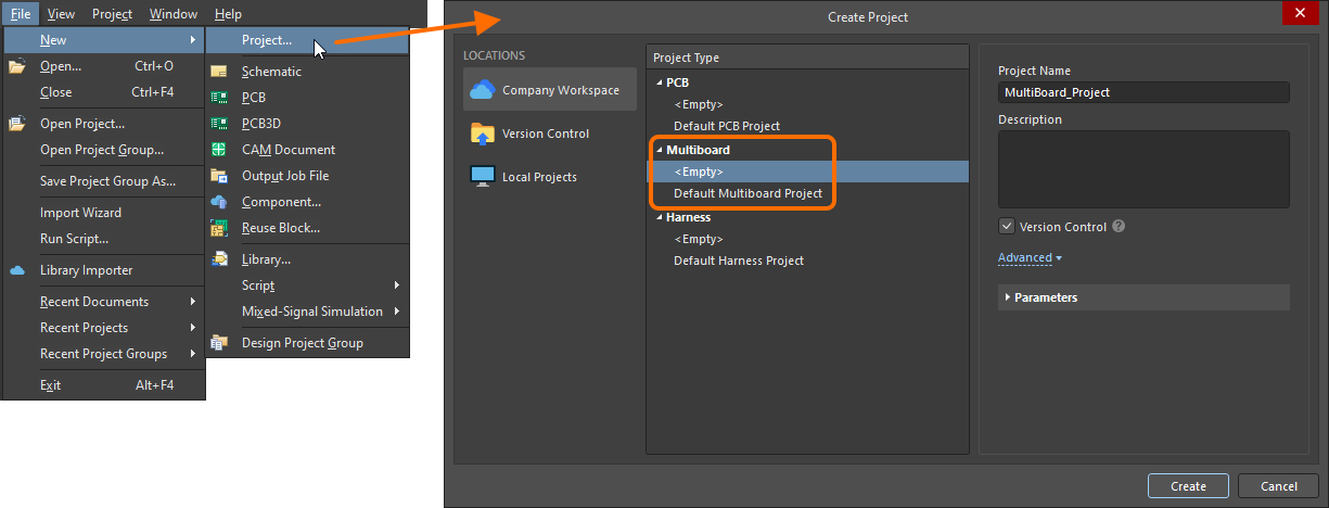
A multi-board design project supports the following documents:
- Multi-board Schematic (
*.MbsDoc) – graphical blocks (modules) that represent the child PCB projects are placed and connected to each other to create the logical system design.
- Multi-board Assembly (
*.MbaDoc) – PCBs referenced by modules in the multi-board schematic are loaded to the multi-board assembly document, where you can position each board (along with an enclosure if needed).
- ActiveBOM (
*.BomDoc) – contains a BOM list of components used in child PCB projects.
- Draftsman Document (
*.MbDwf) – views of the multi-board assembly are imported and annotated, and any additional information required to manufacture the design is added.
-
Output Job File (*.OutJob) – a set of required outputs for your multi-board design can be pre-configured using an Output Job file. Each output is configured with its own settings and its own output format, for example, output to a file or to a printer. The same Output Job file configured for a multi-board design project can then be reused between designs, saving time and effort in preparing outputs for each new design.
While Output Job files facilitate streamlined preparation and generation of outputs, your multi-board design outputs can also be generated directly from the project documents (e.g., using the File » Export commands for a multi-board Assembly document or Reports » Bill of Materials command for an ActiveBOM document).
Outputs Supported for a Multi-board DesignExpandCollapse
Documentation Outputs
Report Outputs
-
Bill of Materials
-
BOM Compare
-
Export Comments
Validation Outputs
-
BOM Checks
-
Components states
-
Configuration compliance
Export Outputs
-
MBA Export PARASOLID
-
MBA Export STEP
PostProcess Outputs
- The set of Altium Designer's example projects includes a sample multi-board design project (
MiniPC.PrjMbd in the C:\Users\Public\Documents\Altium\AD<version>\Examples\Mini PC folder by default), so you can take multi-board designs for a test drive straight out of the box. Also, if you're enjoying the benefits of a Workspace, a sample multi-board project (Sample - Kame-1) will be available when connecting to the Workspace (if you opted to include the sample data during activation/installation of the Workspace).
- Multi-board projects and their associated sub-projects can be saved to a connected Workspace, where they can benefit from the version control, sharing and management capabilities provided by an Altium 365 Workspace or Enterprise Server Workspace. See Sharing a Multi-board Project for information on storing and sharing a multi-board project in an Altium 365 Workspace.
Capturing the Logical System Design
To start capturing the schematic for your multi-board design, add a new multi-board schematic document to the multi-board project. To do this, right-click the project's entry in the Projects panel and select Add New to Project » Multi-board Schematic command from the context menu. The default multi-board schematic document will appear in the design space.
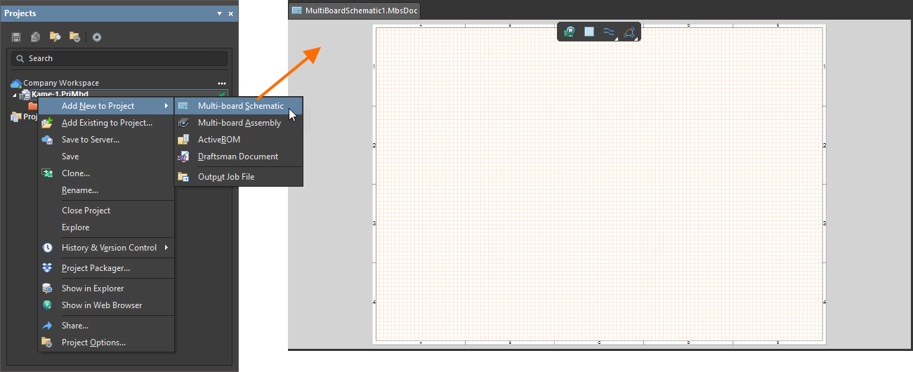
A newly created multi-board schematic document will be the active document in the design space.
Options for a multi-board schematic document are configured in the Properties panel when no object is selected in the design space. The main options are configured on the General tab of the panel:
- Units (the General region) – select the preferred measurement units (mm or mils) for the document.
- Grid and snap settings (the General region) – set the required values for easier navigation and object placement.
- Page options (the Page Options region) – configure the Formatting and Size, as well as Margins and Zones for the document. You can select an available Template, choose a Standard sheet size or define a Custom size.
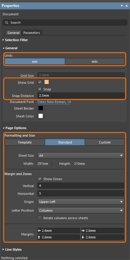
Configure options of the multi-board schematic document in the Properties panel.
To represent a child PCB project design on the multi-board schematic, place a module using the Place » Module command from the main menus. In the Properties panel for the selected module, define its Designator and Title, as well as the source PCB project to which the module is linked. Use the  button associated with the Source field to specify a local or Workspace project and the Assembly/Board drop-down to select the desired PCB within that project.
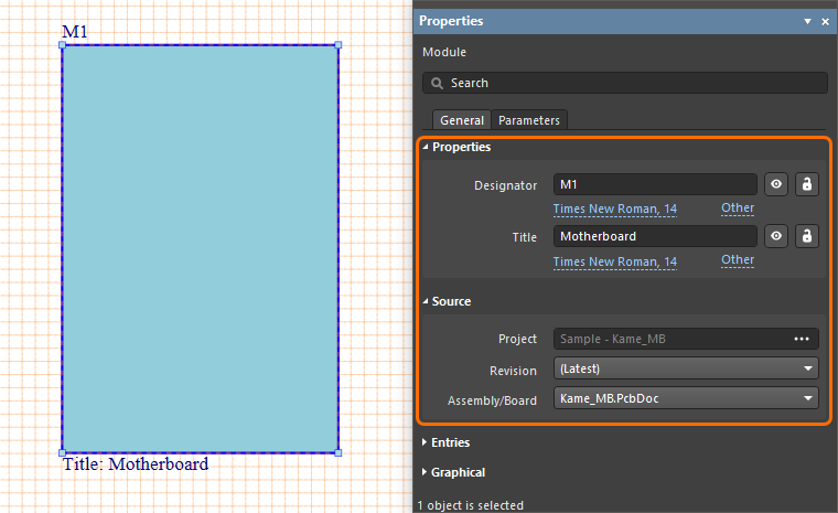
Configure the source and other properties of a module in the Properties panel.
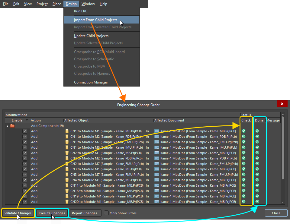
Import the design data from projects referenced by placed modules using the Design » Import From Child Projects command from the main menus. The Engineering Change Order dialog will open presenting the list of changes (Engineering Change Order – ECO) required to synchronize connectivity data in the multi-board schematics with the child projects.
- By default, all modifications are enabled for inclusion when the ECO is executed. You can enable/disable modification entries as required.
- Click the Validate Changes button to run a validation check on the modifications enabled for inclusion in the ECO. Validation results will appear in the Check column in the Status region of the dialog.
- When you are satisfied with the changes to be performed, click the Execute Changes button to execute the ECO and effect the valid changes contained therein. Execution results will appear in the Done column in the Status region of the dialog.
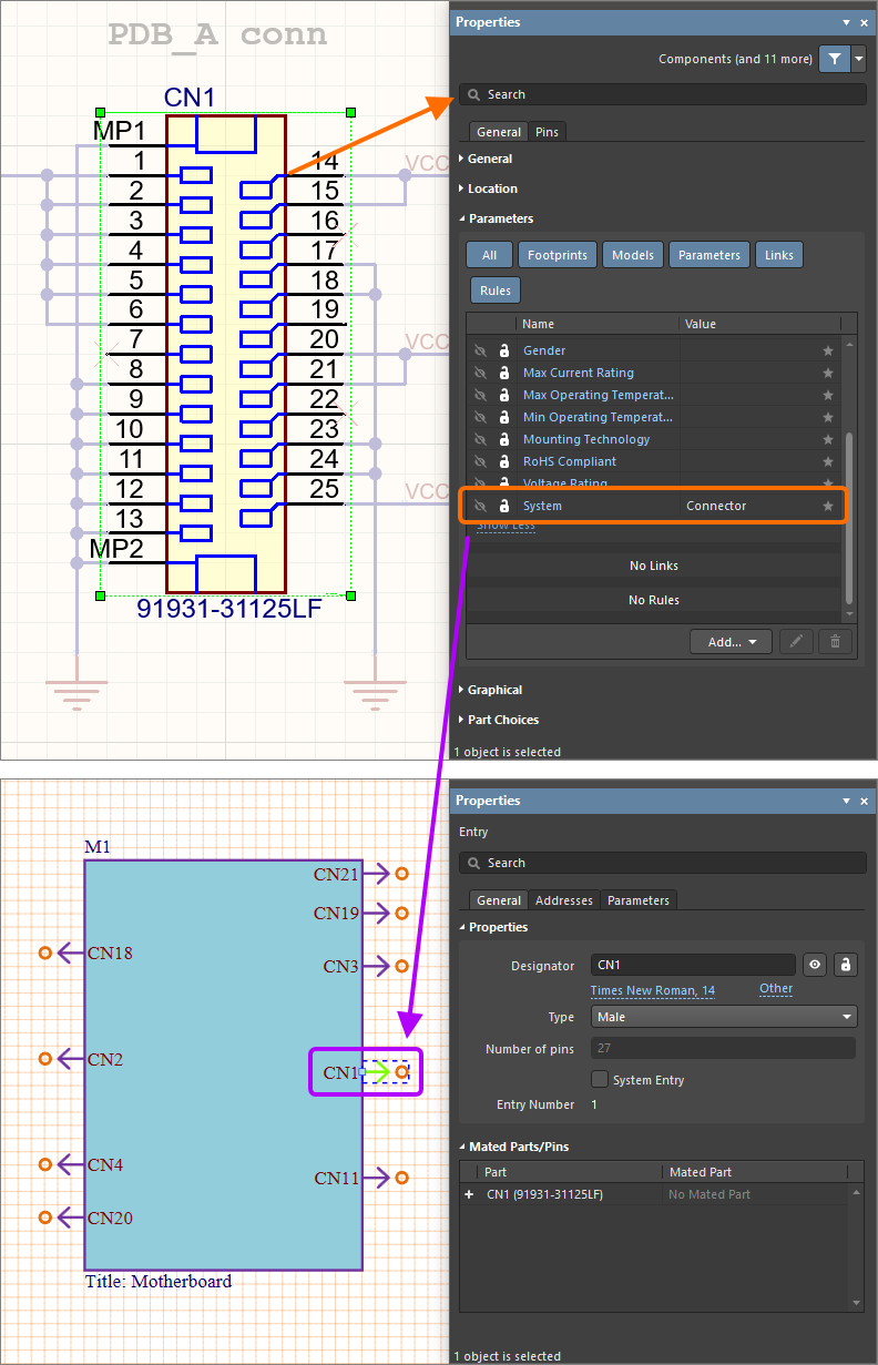
When executing the ECO, a module entry for each connector is created in the respective module. A component in a child PCB project is considered a connector for a multi-board design if it has a parameter named System, with Connector as the parameter value.
To represent the connectivity between child projects, their modules are connected to each other on the multi-board schematic using connections of different types. Select the Direct Connection, Wire, Cable or Harness command from the Place main menu then drag the connection line between hotspots of module entries.
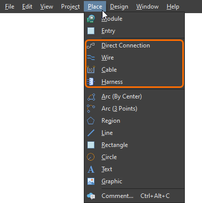
Place connections using commands from the Place main menu.
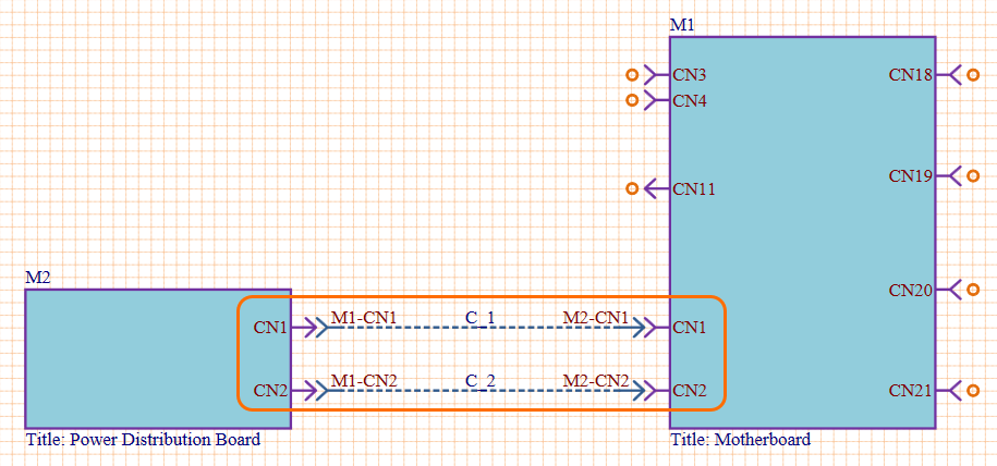
Two modules have been connected by placing two Direct Connections between their module entries.
Select a connection line to show and edit relevant options of the connection in the Properties panel.
To validate the multi-board design, choose the Design » Run ERC command from the main menus. The design will be checked against the settings configured on the Error Reporting tab of the Project Options dialog accessed by right-clicking the project entry in the Projects panel and selecting Project Options. Detected violations will be listed in the Messages panel.
Note that the Messages panel will only open automatically if there is at least one Error or Fatal Error violation. To check for a Warning, open the panel manually (click the Panels button on the bottom-right of the design space, then choose Messages).
- Use the Connection Manager dialog (Design » Connection Manager) to explore the overall connectivity in a multi-board design and resolve detected connectivity issues.
- Use the Design » Import From Child Projects command from the main menus to bring the changes made in child PCB designs into the multi-board design.
Creating the Physical Multi-board Assembly
Once the logical structure of the system is defined in a multi-board schematic, the physical multi-board design is then created by positioning boards in a multi-board assembly.
To add a new multi-board assembly document to your multi-board design, right-click the project's entry in the Projects panel and select Add New to Project » Multi-board Assembly command from the context menu. The default multi-board assembly document will appear in the design space.
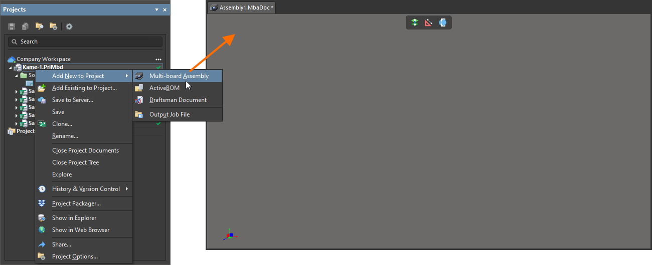
A newly created multi-board assembly document will be the active document in the design space.
To load the PCB referenced by each module in the multi-board schematic into the multi-board assembly, use the Design » Update Assembly - <MultiBoardAssemblyDocumentName> command from the main menus of the multi-board schematic editor. The Engineering Change Order dialog will open presenting the list of changes required to add the PCBs to the assembly. Click the Validate Changes button to run a validation check on the modifications enabled for inclusion in the ECO, then click the Execute Changes button to execute the ECO and effect the valid changes contained therein.
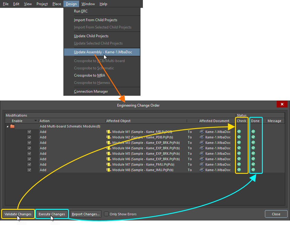
When the Execute Changes button is clicked, the PCBs are loaded into the multi-board assembly editor, and the Engineering Change Order dialog can be closed.
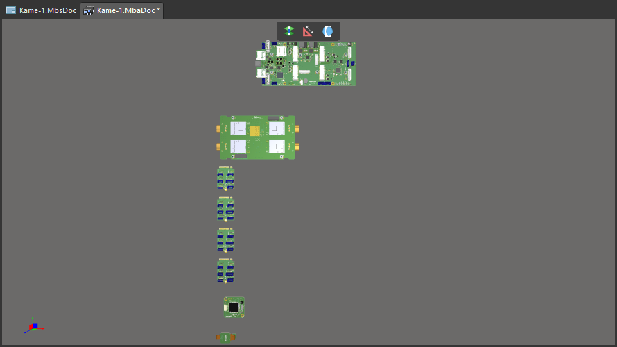
A multi-board assembly after updating from the multi-board schematic.
Use the following shortcuts to navigate the multi-board assembly:
- Ctrl+Mouse Wheel – zoom in and out
- Right-Click, Hold&Drag – pan
- Shift + Right-Click, Hold&Drag – rotate
You can also use the gizmo at the bottom left of the design space to orient the view along the main axes by clicking the arrows and planes of the gizmo.
To position and orient a PCB in the assembly, select it and use the arrows and arcs of the object gizmo that appear to move and rotate the PCB in corresponding directions.
To manipulate two PCBs as a single object, you can create a mate at a selected point on a surface on each of them. To mate two PCBs:
- Select the Tools » Mating command from the main menus.
- Hover the cursor over a planar or cylindrical surface of the target PCB and select a point on it to define the first mate site.
- Hover the cursor over a planar or cylindrical surface of the source PCB and select a point on it to define the second mate site. The source PCB will move so that the source site and the target site are mated (located together), with their surface planes and perpendicular axes aligned.
- Use the Properties panel or shortcuts listed in the panel to adjust the mate settings.
STEP models can be loaded to a multi-board assembly to complete it with an enclosure/case or other mechanical parts, for example. Use the Design » Insert STEP Part command from the main menus to add a STEP model.
❯ ❮
Javascript ID: MBA_STEP
|
To check a multi-board assembly for collisions (situations where two objects have surfaces that touch or intersect), select the Tools » Check Collisions command from the main menus. Any collisions will be reported through the Messages panel and highlighted in the design space. Note that mated surfaces are not considered to be colliding.
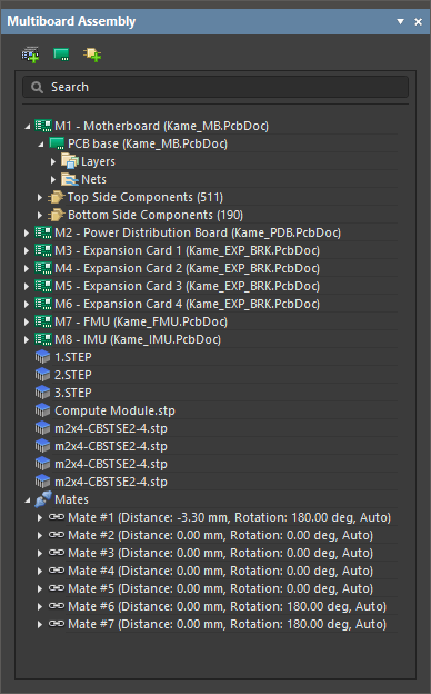
The Multiboard Assembly panel presents a tree view of the assembly structure and includes all PCBs in the assembly, as well as any created mates and added STEP models. Use the tree and right-click menu commands of entries to navigate and manage the multi-board assembly.
Creating a Manufacturing Drawing
Once the multi-board assembly is complete, a manufacturing drawing can be created and annotated. A manufacturing drawing for a multi-board design is being created in the Draftsman editor.
To add a new multi-board assembly document to your multi-board design, right-click the project's entry in the Projects panel and select Add New to Project » Draftsman Document command from the context menu. The New Document dialog opens from where you can select a predefined document template or the [Default] option that creates a blank A4 document. After clicking OK, a new Draftsman document will appear in the design space.
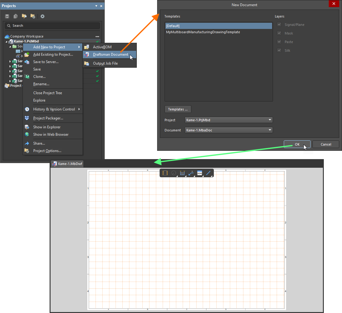
A newly created Draftsman document will be the active document in the design space.
- Options for the Draftsman document, such as the Sheet Size, are configured in the Properties panel when no object is selected in the design space.
- Draftsman extracts design data directly from the multi-board assembly document. When the multi-board assembly data has changed, you can refresh the data in Draftsman by selecting the Tools » Import Changes From <MultiBoardAssemblyDocumentName>.MbaDoc command from the main menus.
In a manufacturing drawing of a Multi-board design project, the following views are available:
- Multi-board view – an automated graphic composite of the outlines of PCBs and 3D models constituting the multi-board assembly.
- Section view – a profile slice, or sectional, drawing taken from a nominated 'cut' point through a placed multi-board view.
- Board detail view – a floating, magnified view of a multi-board view's defined area.
- Board realistic view – a scalable 3D rendering of the current multi-board assembly.
To place a drawing view, select a command for the required view type from the Draftsman editor's Place menu: Multiboard View or a command from the Additional View menu.
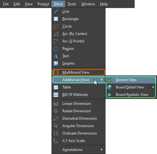
Place drawing views using commands from the Place main menu.
- After selecting the Multiboard View or Board Realistic View command, you will enter the placement mode indicated by a crosshair and the view under the cursor. Click in the design space to place the view.
- After selecting the Section View or a Board Detail View command, define the position of the cut line or the detail view area on a placed multi-board view, respectively.
When a drawing view is placed, its properties can be configured in the Properties panel when the view is selected in the design space.
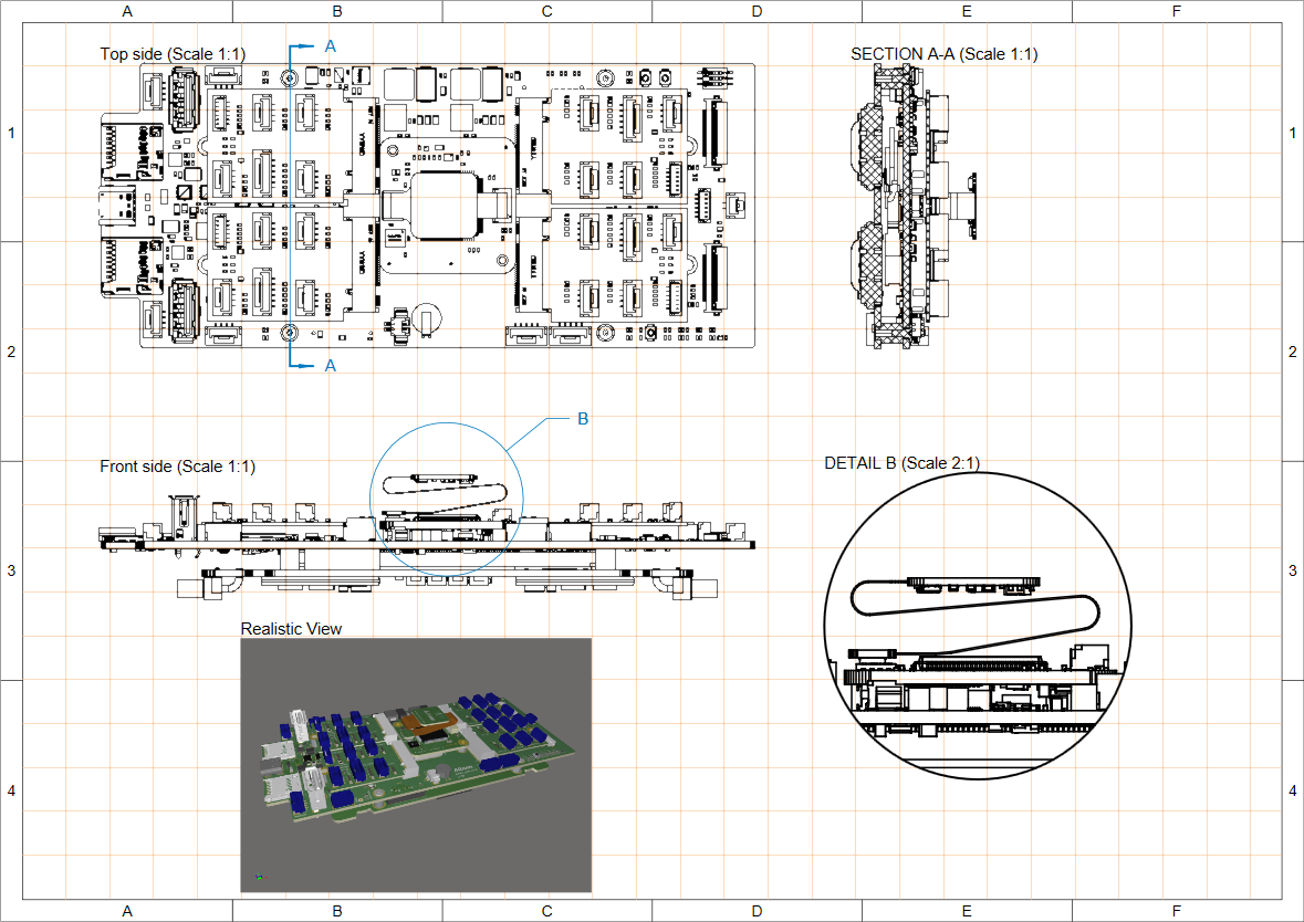
A sheet of a Draftsman document with some placed views: two multi-board views, a section view, a board detail view, and a board realistic view.
To add important details to drawings, Draftsman provides additional annotation, dimensioning and table tools:
- To indicate the lengths, sizes, and angles of the object outlines or the distance between objects, dimension graphics may be placed on board views. Use the group of dimension placement commands in the Place main menu to select the required dimension type.
- To add important information to your drawings, additional annotation tools, such as callout, surface finish indicator and automated note list, are provided. Use the commands of the Place » Annotation menu from the main menus to select the required annotation tool.
- To add Bill of Materials (BOM) data to the manufacturing drawing, a Bill of Materials table (Place » Bill Of Materials) can be placed. The Bill of Materials table will draw data from and reflect an ActiveBOM document added to the Multi-board design project. Also, a generic Table that can be filled with custom data is available (Place » Table).
- To place basic, free-form drawing elements in a drawing document, a range of graphical element tools is also provided. Use the group of graphical object placement commands in the Place main menu to select the required object type.