This page details the improvements included in the initial release of Altium Designer 24, as well as those added in subsequent updates. Along with delivering a range of improvements that develop and mature the existing technologies, each update also incorporates a large number of fixes and enhancements across the software based on feedback raised by customers through the AltiumLive Community's BugCrunch system, helping you continue to create cutting-edge electronics technology.
You can choose to continue with your current version, update your current version, or install Altium Designer 24 alongside your current version to access the latest features. Your current version can be updated from within the software in the
Extensions and Updates view. If you prefer to install Altium Designer 24 alongside your current version, visit the
Altium Downloads page to download the installer, then choose
New Installation on the
Installation Mode page of the installer.
Free Trial!
If you like what you see but are not yet a customer, why not take Altium Designer for a test drive? By filling out a simple form, you can try Altium Designer for free with 15 days of access to the full software. That's right, you will have the ability to evaluate the full Altium Designer experience with no technical limitations with unfettered access to the world's finest PCB design product. Click the link below, fill out the form, and see for yourself why more engineers and designers choose Altium than any other product available!
Altium Designer Free Trial.
Altium Designer 24.3
Released: 19 March 2024 – Version 24.3.1 (build 35)
Release Notes for Altium Designer 24.3.1
PCB Design Improvements
Pad Corner Radius/Chamfer as an Absolute Value (Open Beta)
In this release, the ability to define pad corner radius/chamfer as an absolute value (in mil or mm) has been added.
When a pad of the Rounded Rectangle or Chamfered Rectangle shape (on a copper, paste or solder layer) is selected in the PCB or PCB Footprint editor, enter a value to the Corner Radius field to define the radius/chamfer as an absolute value (with the default measurement units). Note that the absolute value of the pad corner radius/chamfer must be less than or equal to half of the shortest pad side. The calculated percentage value will be shown at the right of the field.
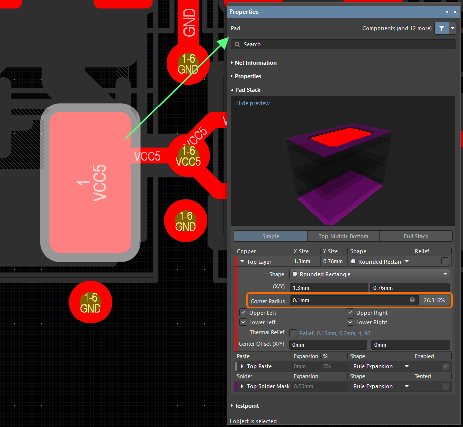
Enter a value to the Corner Radius field to define it as an absolute value.
Enter a value followed by the % symbol to define the radius/chamfer as the percentage of half of the pad's shortest side (as in previous versions).
The absolute value of the pad corner radius chamfer is also supported by the PCB List and PCBLIB List panels, the Find Similar Objects dialog, and the Pad/Via Template editor. Also, the following query keywords can now be used in expressions:
| Keyword |
Summary |
|
Pad_CornerRadius_Value_AllLayers
Pad_CornerRadius_Value_TopLayer
Pad_CornerRadius_Value_BottomLayer
Pad_CornerRadius_Value_MidLayer<n>
(where n = 1..30)
|
Return pad objects whose Pad Corner Radius Size property for the corresponding layer complies with the query.
For example, the AsMM(Pad_CornerRadius_Value_TopLayer) > '0.1' query returns pad objects whose Pad Corner Radius Size (Top Layer) property is greater than 0.1mm.
|
|
Pad_CornerRadius_UsesPercent_AllLayers
Pad_CornerRadius_UsesPercent_TopLayer
Pad_CornerRadius_UsesPercent_BottomLayer
Pad_CornerRadius_UsesPercent_MidLayer<n>
(where n = 1..30)
|
Return pad objects whose Pad Corner Radius Uses Percent property for the corresponding layer complies with the query.
For example, the Pad_CornerRadius_UsesPercent_MidLayer2 = 'False' query returns pad objects whose Pad Corner Radius Uses Percent (Mid Layer 2) property is disabled (i.e. an absolute value is used to define the pad radius on this layer).
|
Note that the existing Pad_CornerRadius_AllLayers, Pad_CornerRadius_TopLayer, Pad_CornerRadius_BottomLayer and Pad_CornerRadius_MidLayer<n> (where n = 1..30) are still used to scope pad objects whose Pad Corner Radius (%) property for the corresponding layer complies with the query.
Support for pad corner radius/chamfer defined as an absolute value has also been added to the Import Wizard when importing an Xpedition design.
This feature is in Open Beta and available when the
PCB.Pad.CustomShape.CornerRadiusAbsolute option is enabled in the
Advanced Settings dialog.
PCB Replication Improvements
Enhanced Error Notifications
If a missing pin connection in the selected Source Block is detected when running the Layout Replication tool, the warning dialog will notify you about the missing connection.
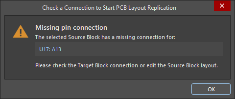
Click the link in the dialog to cross-probe to the offending object.
Added 'Busy' State for PCB Replication
To provide a more responsive UI for the PCB replication process, the indicators of the feature 'busy' state were added in this release.
-
When running the Layout Replication tool, an indication that replication data is loading, with the possibility to cancel out of the process, appears before opening the PCB Layout Replication dialog.
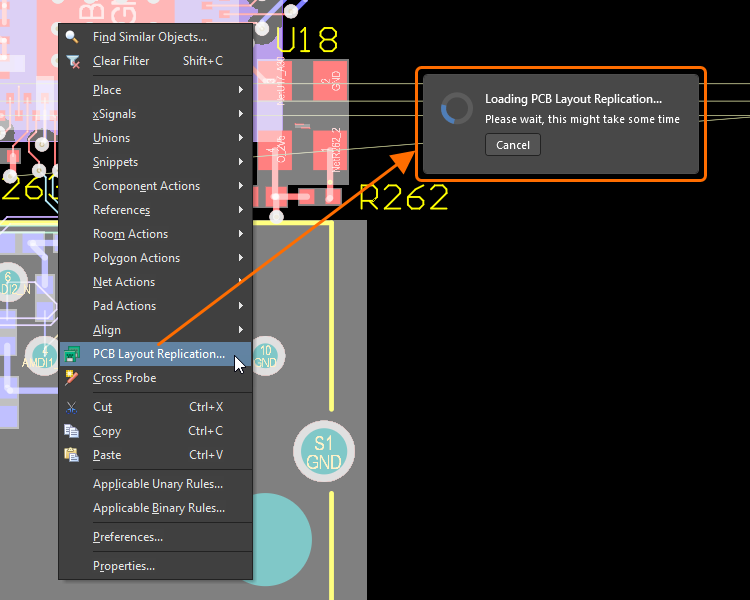
- After clicking the Replicate button in the PCB Layout Replication dialog, the cursor indicates 'in progress' (
 ) before the first block is placed (or ready for placement in interactive mode).
Constraint Manager Improvements
Added Support for Importing Design Directives (Open Beta)
You can now import constraints from design directives, placed and defined on your schematic source documents, into the Constraint Manager. This is performed from the Physical or Electrical view (when accessing the Constraint Manager from a schematic) using the new Import from Directives command (from the right-click context menu) and supports rule, net class, diff pair, and diff pair class directives.
Note that any existing constraints already defined for nets/net classes/diff pairs/diff pair classes through the Constraint Manager will take precedence and are, therefore, kept when an import is processed.
❯ ❮
Javascript ID: CM_ImportDirectives_AD24_3
|
On a schematic, some Parameter Set and Differential Pair directives are placed. These directives define a diff pair, a net class and Width rules.
Use the Import from Directives command from the right-click menu in the Constraint Manager.
The data from the directives will be imported into the Constraint Manager.
|
This feature is in Open Beta and available when the
ConstraintManager.ImportFromDirectives option is enabled in the
Advanced Settings dialog.
New 'Diff Pairs' Tab
A new Diff Pairs tab is now available from the Electrical constraints view for explicitly defining and managing differential pairs. A hierarchical list of the differential pairs in the design is shown on this tab. Select a cell for a differential pair or differential pair class to present constraints for it in the bottom region of the Constraint Manager.
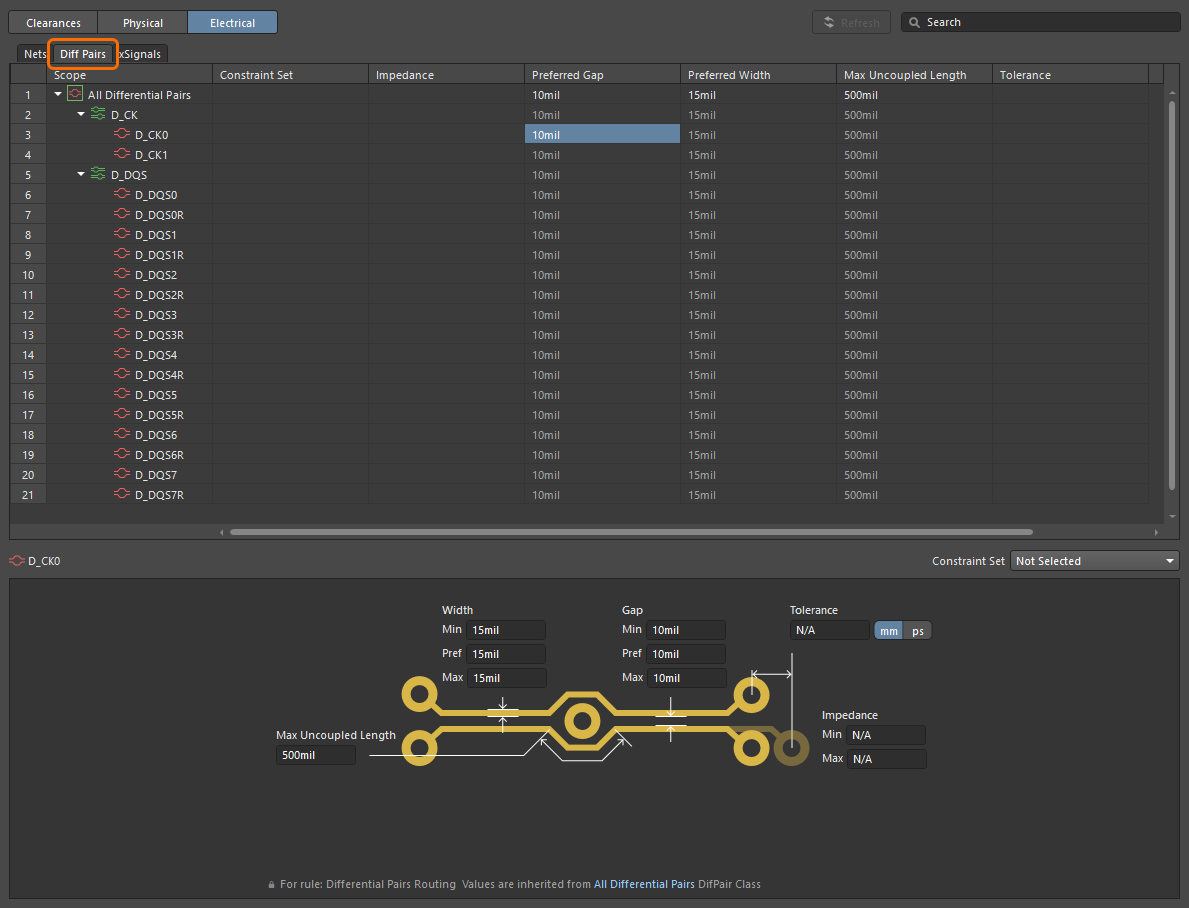
Support for Creepage in the Clearance Matrix
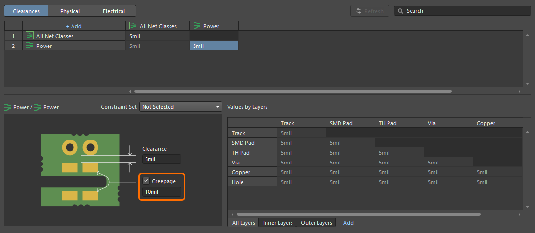
A Creepage rule can now be specified when defining electrical clearances between classes of nets and/or differential pairs using the matrix in the Clearances view.
Support for Multi-editing in the Clearance Matrix
Added support to the clearance matrix (the Clearance view) for multi-editing within a selected row/column. In the detailed clearance settings of the Constraint Manager, select a row or column, type the required value, and press Enter or click to apply this value to all cells of the row/column.
Draftsman Improvement
Ability to Change the Resolution of a Board Realistic View
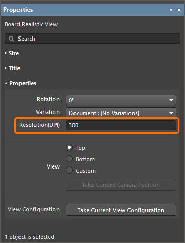
The resolution for a placed Board Realistic View can now be configured in the Resolution(DPI) field in the Properties region of the Properties panel by entering the desired resolution in the field. Previously, the view was a static rendered image with no way to change the resolution. The minimum setting is 75 DPI, and the default setting is 300 DPI.
Harness Design Improvements
Cavity Enhancements
Specifying Cavity Types
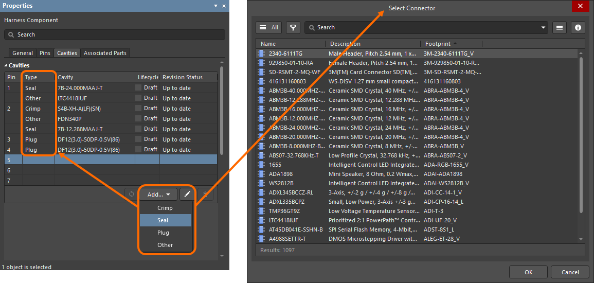
You can now specify the type of cavity for each pin of a harness component in the Wiring Diagram (*.WirDoc). On the Cavities tab of the Properties panel, select the desired pin, then click Add. Choose the cavity type from the drop-down. In the Select Connector dialog that opens, select the specific desired connector for the pin.
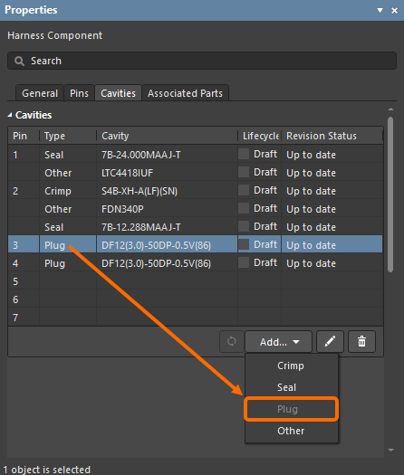
Only one cavity of a particular type can be added to a pin. Once a cavity of a particular type has been added, the entry is unavailable (grayed out) in the drop-down, as shown in the image below for Pin 3.
Added New Cavity Types to Wiring List and Connection Table
Seals, plugs and other cavity parts can be displayed in a wiring list and connection table in a manufacturing drawing. Enable the visibility of the desired columns in the Columns tab of the Properties panel when the placed table is selected in the design space.

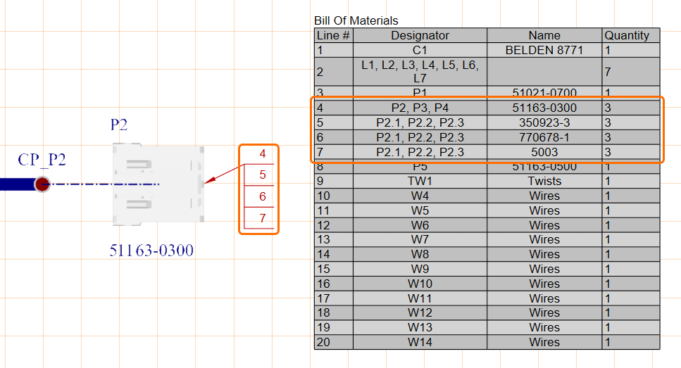
Added Cavity BOM Line Numbers to Callouts on the Manufacturing Drawing
When a callout set to display the BOM Item is added to the physical view of a component on a layout drawing view, it will include BOM line numbers for all assigned cavities.
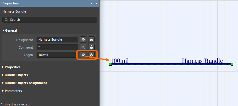
Visibility and Lock Options for Harness Bundle Length Parameter
The Length parameter of a harness bundle in a Layout Drawing (*.LdrDoc) now includes visibility and lock options.
Highlight Bundles with Wires from Split Cables
All harness bundles that include wires from a split harness cable are now highlighted on the Layout Drawing when the cable is selected in the Bundle Objects region of the Properties panel. For a split cable, the length of the longest wire is shown in BOM.
❯ ❮
Javascript ID: HD_SplitCable_AD24_3
|
Cable C1 is split between different connectors.
When clicking the cable entry in the Bundle Objects region of the Properties panel for the selected bundle, all bundles that include wires from C1 are now highlighted.
In BOM, the length of the longest wire (a wire that passes through bundles B1 and B3 in this example) is shown for C1.
|
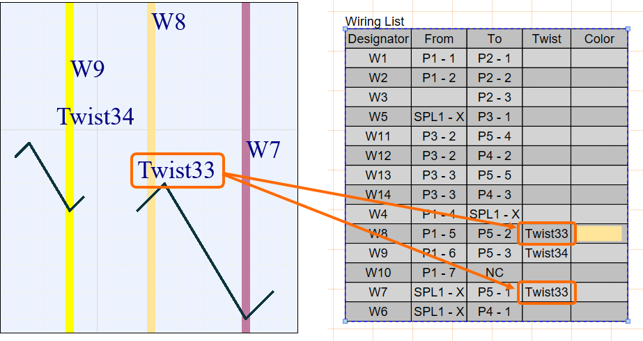
Added Twist Object Designator to the Wiring List
The designator of a twist object is now displayed in the wiring list as shown in the image below.
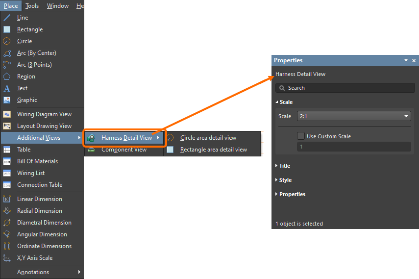
Board Detail View Renamed Harness Detail View
The Board Detail View in a Harness Draftsman document (*.HarDwf) has been renamed Harness Detail View.
Display Individual Wire Lengths in Wiring List and Connection Table
The Length column in a wiring list and connection table now displays the individual wire lengths for each wire in a cable.
❯ ❮
Javascript ID: HD_IndividualWireLength_AD24_3
|
Wires W1, W2 and W3 are part of a cable.
Individual lengths of these wires are now shown in a wiring list and connection table.
|
Display Total Length of Wires and Cables in BOM
For harness wiring components, the Length column in the ActiveBOM document and BOM Table in a manufacturing drawing now presents the total length for wires/cables of the same BOM item rather than their individual lengths.


Data Management Improvements
Support for Custom Pricing
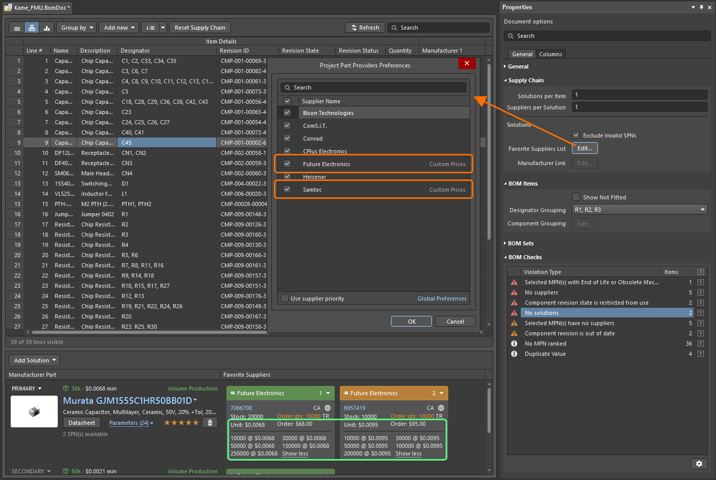
When you have a configured connection to a specific supplier account through the browser interface of your Altium 365 Workspace (learn more), you can now see custom pricing where applicable in the ActiveBOM and all places where part choices are accessed. Also, suppliers that provide custom prices are labeled as such in the Project Part Providers Preferences dialog, which can be accessed by clicking the Edit button in the Favorite Suppliers List field in the Properties panel for the ActiveBOM document.
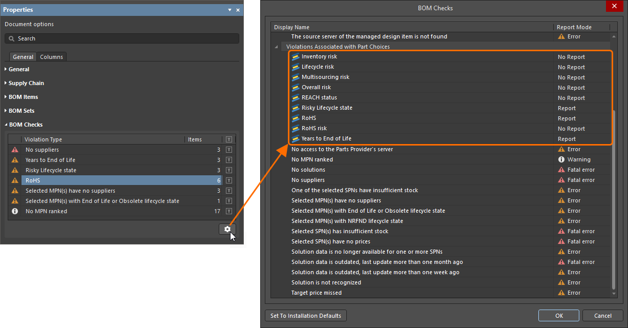
Added BOM Checks for SiliconExpert Parameters
Support for a range of checks based on SiliconExpert parameters was added to ActiveBOM. You can enable or disable these checks in the Violations Associated with Part Choices category in the BOM Checks dialog. Open the dialog by clicking the  button in the BOM Checks region of the Properties panel.
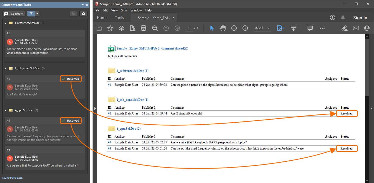
Added Comment Resolved Status to Exported PDF
When exporting comments to PDF, the status for resolved simple comments (i.e., those not assigned as 'tasks') is now included in the export.
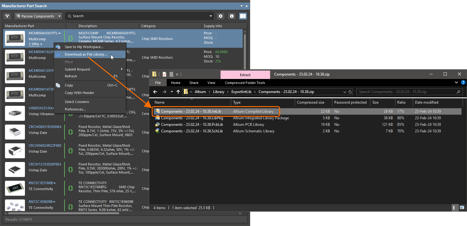
Added Compiled IntLib to Downloaded Manufacturer Part Zip
When downloading a component from the Manufacturer Part Search panel as a file library, the compiled Integrated library (*.IntLib) is now included as part of the Zip file.
Import/Export Improvement
Xpedition Library Import Enhancements
This release adds the following improvements when importing an Xpedition library into Altium Designer.
- Added support for 'Round Donut' pad shapes defined in footprints within an Xpedition library. Note that this first step enables such footprint pads to be imported (as custom pad shapes). There is no dedicated ‘Round Donut’ pad shape in PCB/PCB Footprint editors.
- Defined pad hole tolerances are now included when importing an Xpedition library.
- Added support for replicated text strings in footprints (i.e., mounting hole 'A's) when importing an Xpedition library. The original string, its replicates, and associated parameters are imported.
- Added support for zero-width lines defined for a footprint on the Placement Outline layer when importing an Xpedition library.
Circuit Simulation Improvements
Simulation S-Parameters Analysis (Open Beta)
This release adds the ability to run an analysis of S-parameters (scattering parameters). Such parameters facilitate an approach for describing networks based on the ratio of incident and reflected microwaves (for a device under test, how much power passes from one port to another, and how much power is reflected back). These ratios can be subsequently used to calculate the properties of a circuit, including input impedance, frequency response and isolation. While this type of analysis is primarily for RF circuits and components, it is equally useful for any circuit with at least two sources (ports).
This new analysis is done by enabling the S-Parameters Analysis option in the AC Sweep region of the Simulation Dashboard panel. Define the ports (sources) involved and set an impedance for each (default is 50 ohms). If a device has more than two ports, these can be added and defined accordingly, which will result in more S-parameters involved in the resulting ‘S-matrix.’ Once the AC sweep analysis is run, the S-parameters data will be available on the S-parameters Analysis chart in the SDF document.
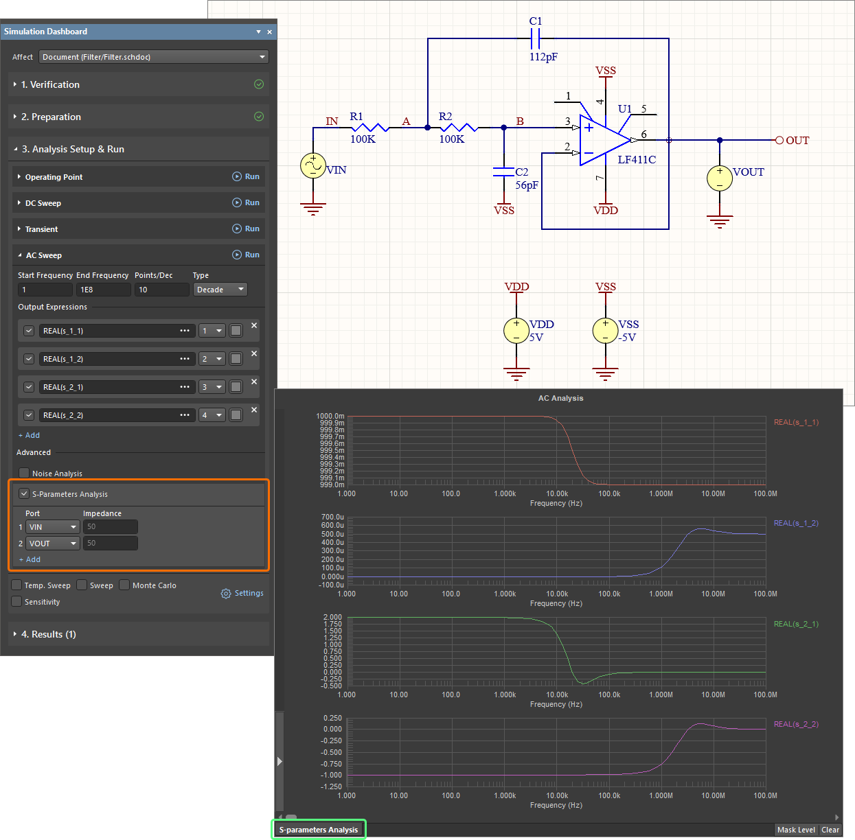
The simulation engine also calculates Y-parameters (admittance) and Z-parameters (impedance), which can be added to plots in the chart as desired.
This feature is in Open Beta and available when the
Simulation.SParametersAnalysis option is enabled in the
Advanced Settings dialog.
Added Ability to Present SPICE Models in the Components Panel
In this release, a new Show in Components Panel option has been added to the Simulation – General page of the Preferences dialog. When this option is enabled, the SPICE Libraries category is available in the Components panel, and the libraries contained in the Model Path folder specified on the Simulation – General page of the Preferences dialog are listed in this category. The category structure reflects the structure of the specified folder.
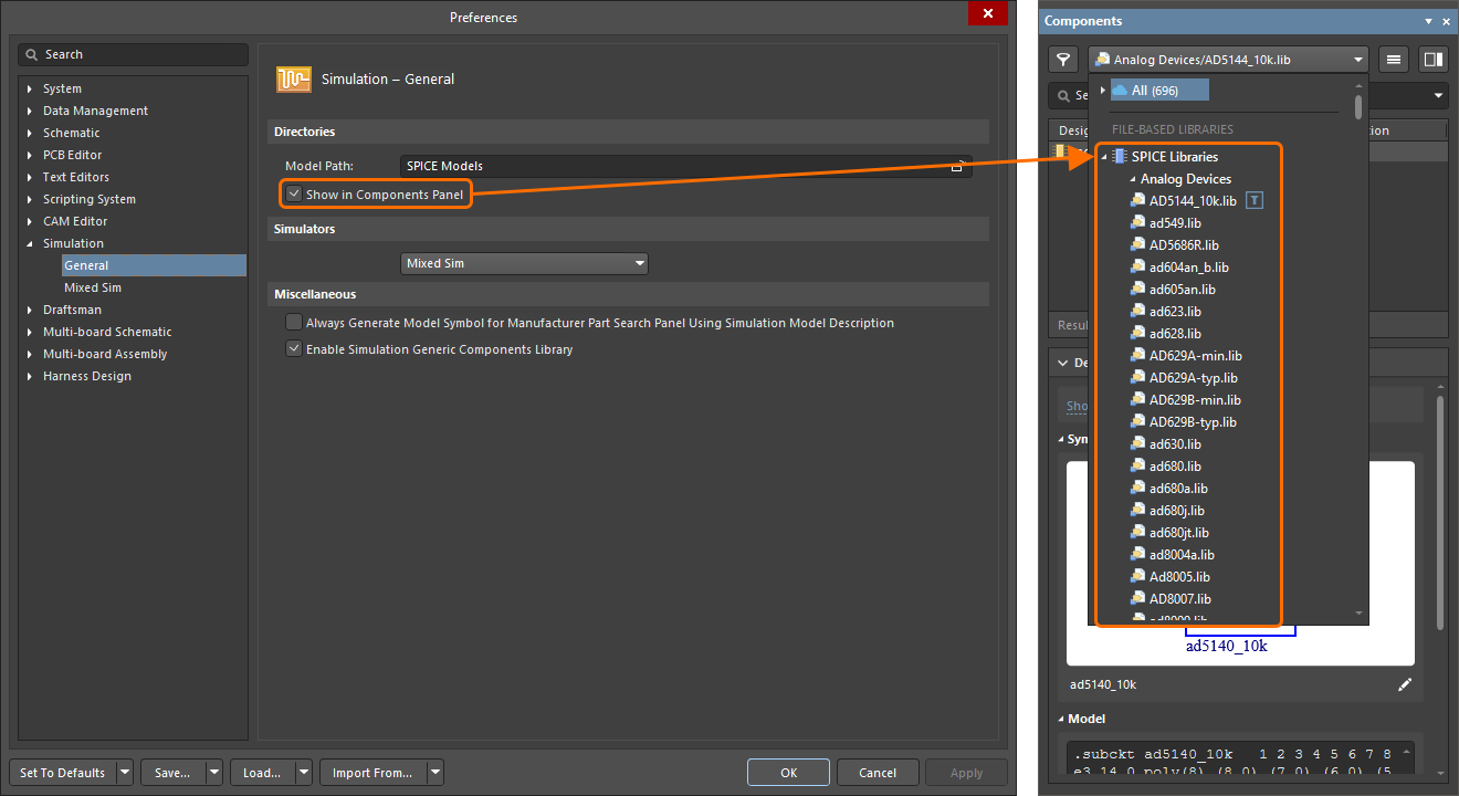
As part of this, a folder of Analog Devices' SPICE models has been added to the Mixed Simulation extension's default installation Library folder (\ProgramData\Altium\Altium Designer <GUID>\Extensions\Mixed Simulation\Library\SPICE Models\Analog Devices).
Added Enable Simulation Generic Components Library Option
A new Enable Simulation Generic Components Library option has been added to the Simulation – General page of the Preferences dialog, allowing you to control the library’s visibility within the Components panel.
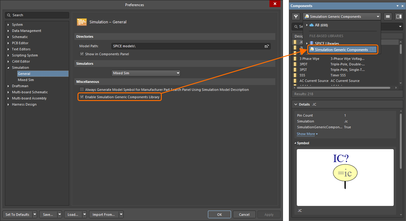
In addition, the library has been removed from the Installed tab of the Libraries Preferences dialog.
Added Support for the 'TEMP' Keyword in Constant Parameters
For temperature analysis, the keyword TEMP can now be used in constant parameters.
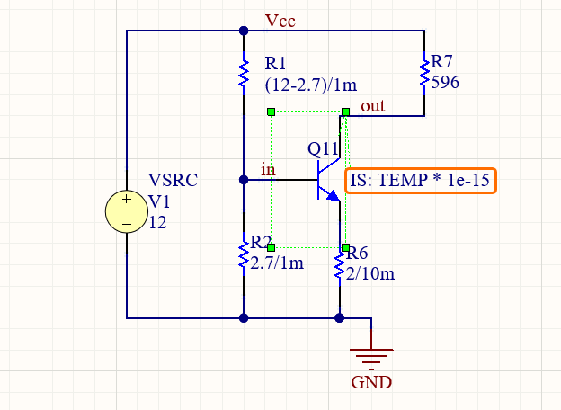
The keyword TEMP can be used in constant parameters. The image shows the TEMP keyword being used to calculate the IS parameter of transistor Q11.
The TEMP value (the actual operating temperature of the circuit in °C) is set on the Advanced tab of the Advanced Analysis Settings dialog accessed by clicking Settings in the Analysis Setup & Run region of the Simulation Dashboard panel.
Note that if the
TEMP keyword is used in a constant parameter, the simulator will not be able to perform a
DC Sweep analysis when the
Temp parameter is selected as a parameter to be stepped for this analysis.
Added Support for the LTspice 'AKO' Model Keyword
When creating a model based on another model, you can now use the AKO model keyword.
In the example shown below, model QP has all the same parameters as model QP350, except that BF is changed and VA is set.
.MODEL QP350 PNP(IS=1.4E-15 BF=70 CJE=.012P CJC=.06P RE=20 RB=350 RC=200)
.MODEL QP AKO:QP350 PNP(BF=150 VA=100)
Error detection is applied when using the AKO syntax, in cases where the model definition involves:
Features Made Fully Public in Altium Designer 24.3
The following features are now officially Public with this release:
Altium Designer 24.2
Released: 15 February 2024 – Version 24.2.2 (build 26)
Release Notes for Altium Designer 24.2.2
Key HighlightsExpandСвернуть
PCB Design Improvements
Added the Ability to Choose Components Manually while Replicating
This release extends the functionality of the PCB Layout Replication tool with the ability to manually map components in target blocks where multiple components have been detected by the tool as having similar connections. This allows you to manually choose between available components that are able to replace each other faithfully without violating circuit connectivity.
When multiple components with similar connections are detected by the tool, corresponding target blocks in the PCB Layout Replication dialog will have the  icon (when the block is collapsed), and each component with available replacements will have the
  icon (when the block is expanded). Use the drop-down in the Designator field of the component with detected replacements to choose the required component.
❯ ❮
Javascript ID: Dlg_PCBLayoutReplication_Alternate_AD24_2
|
Added Differential Pair Common Mode Impedance in Layer Stack Manager
When Differential is selected as the Type in the Properties panel to define an Impedance Profile for a differential pair, a field has been added that shows the common mode impedance for the selected Impedance Profile. This value, which is displayed as Impedance (Zcomm), is taken from Simbeor's calculated transmission line data.

Use of Tuning Miter Parameter for Connecting an Accordion to a Route
When interactively tuning the length of a route by adding an accordion, the Miter parameter defined for the accordion in the Properties panel is now also used to miter the traces that connect the accordion to the route. Previously, the Miter Ratio parameter defined for the interactive routing was used for these traces.
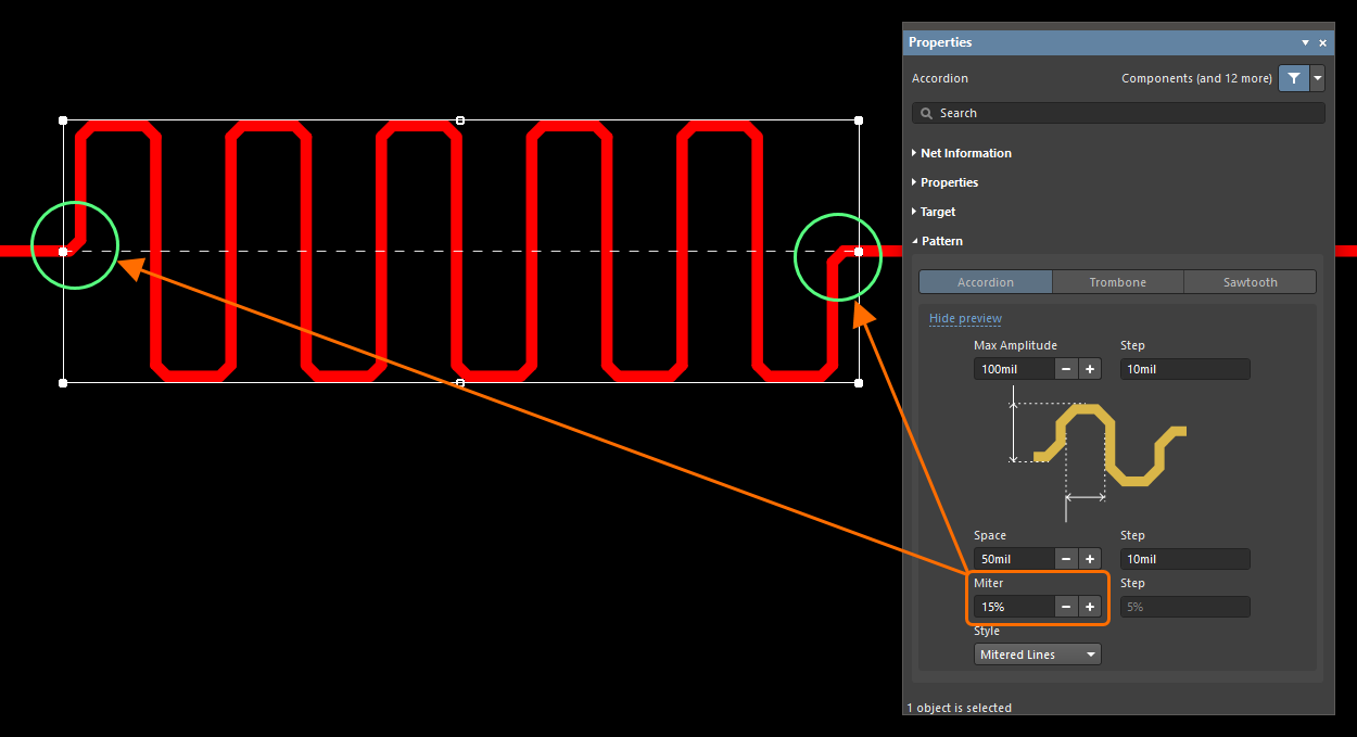
The Miter value from the accordion properties is now also applied to traces connecting that accordion to the route.
Constraint Manager Improvement
Enhanced Ability to Transfer Constraints from PCB to Schematic
In this release, the ability to transfer constraints defined on the Physical and Electrical views of the Constraint Manager has been added. In the PCB editor, select the Design » Update Schematics in <PCBProjectName> command from the main menus and use the Engineering Change Order dialog that opens to explore, validate and execute the changes in constraints.
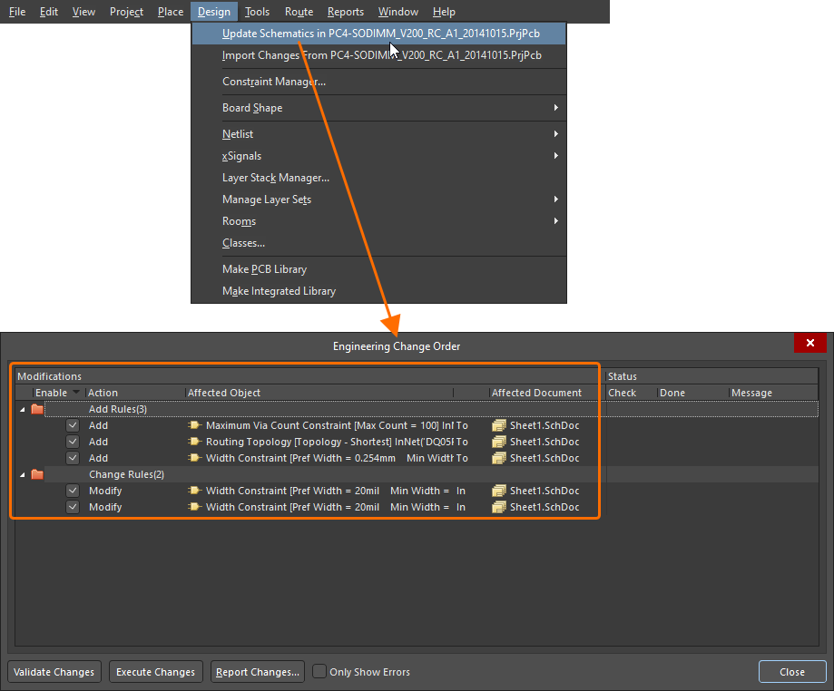
Multi-board Design Improvement
Added Bookmarks Panel for Multi-board Draftsman Documents
The Bookmarks panel is now available in Draftsman when working with a manufacturing drawing of a multi-board design (*.MbDwf). The panel gives a tree view of the sheets on the Draftsman document. Each sheet entry can be expanded and collapsed; when expanded, the appropriate contents of each sheet are displayed as shown in the image below.
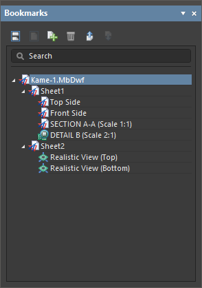
You can use the panel to easily navigate in the design space. When an item is selected in the panel or design space, the Properties panel (if open) displays the properties and settings of the selected item. Additionally, when you select an item in the Bookmarks panel, the design space zooms to the selected item.
Harness Design Improvements
Duplicate Designator Violation Removed for Cable, Shield and Twist Objects
On the Wiring Diagram, the Duplicate Designator (WD) violation check does not report an issue when Cable/Shield/Twist objects use the same designator. This can now be split and used in different places using the same designator.
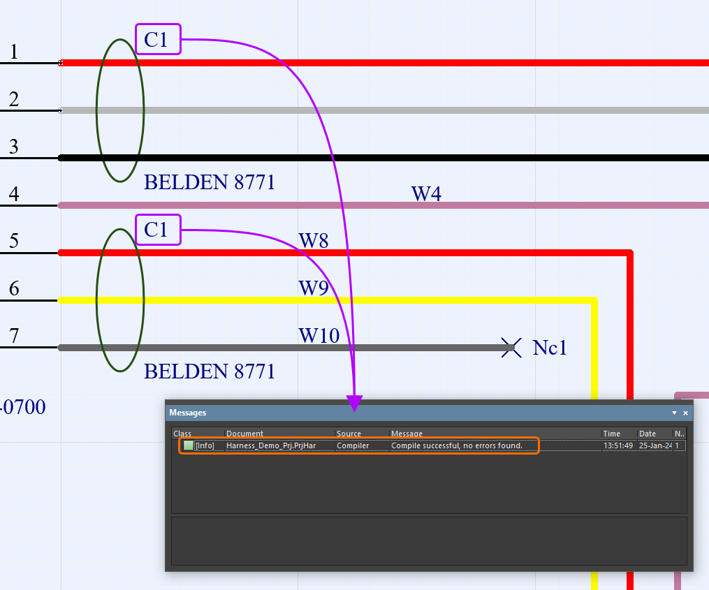
Highlight Wires for Twists and Shields
If a twist/shield is associated with wires in multiple places on the Wiring Diagram (using the same designator), selecting a twist/shield instance will highlight all associated wires in the group with a neon green color.
❯ ❮
Javascript ID: Harness_WD_Highlight
|
An example of a Wiring Diagram where two twists with the same designator are placed on different groups of wires. While only one of these twists is selected, all wires covered by these twists are highlighted.
An example of a Wiring Diagram where two shields with the same designator are placed on different groups of wires. While only one of these shields is selected, all wires covered by these shields are highlighted.
|
Added Support for Multi-part Components
The ability to transfer multi-part component data from the Wiring Diagram to the Layout Drawing has been added. When multi-part components are placed on the Wiring Diagram, designators are correctly assigned to the components in the Layout Drawing. If multiple parts of the same component are placed on the Wiring Diagram, only one instance of the component is placed on the Layout Drawing.
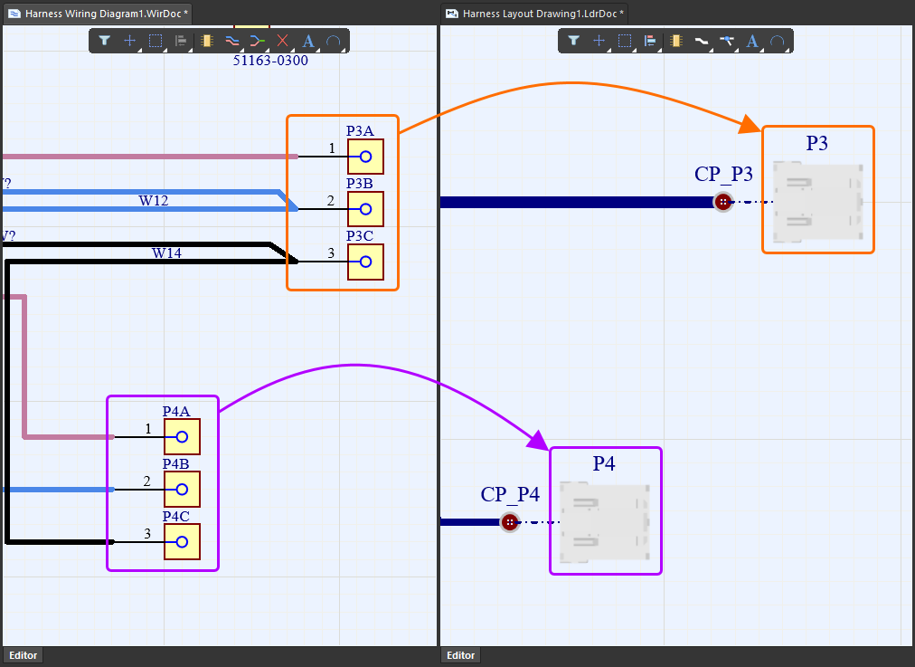
Added Support to Connect Shields to a Connection Point
A shield with a connection object that is defined on the Wiring Diagram can now be assigned to a connection point in the Layout Drawing. Use the Add Assigned Objects dialog (accessed by clicking the Add button in the Assigned Objects region of the Properties panel) when the connection point is selected to choose the shield with a connection to be assigned to that connection point.
❯ ❮
Javascript ID: Harness_ShieldConnection_CP
|
Added Support for Multicolored Wires
Multicolored wires are now supported in the Wiring Diagram by choosing a wire's secondary and tertiary colors. (The primary color is the color of the placed wire.) In the Properties panel, click the Add drop-down at the bottom of the Parameters region then choose Secondary and Tertiary to define the desired colors; the parameter for the chosen color will appear in the Parameters region. Click the color icon in the panel to open the color options; click the desired color. You can also define the border color for the wire using the same drop-down then selecting Border. Click through the slideshow below for examples.
❯ ❮
Javascript ID: MultiColorWire
|
Wire with the secondary color defined
Wire with the tertiary color defined
Wire with the border color defined
Wire with all color options defined
|
Multicolored wires are also supported in harness design Draftsman documents (*.HarDwf). Additional columns for secondary, tertiary and border colors can be made visible in placed tables, and corresponding Color cells are split to show the secondary and tertiary colors assigned to the wire.
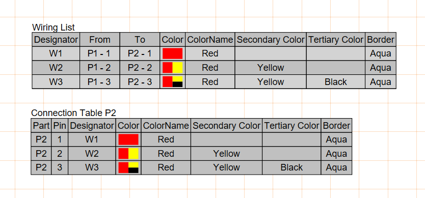
Added Support for Multiple Wiring Diagrams in Draftsman Documents
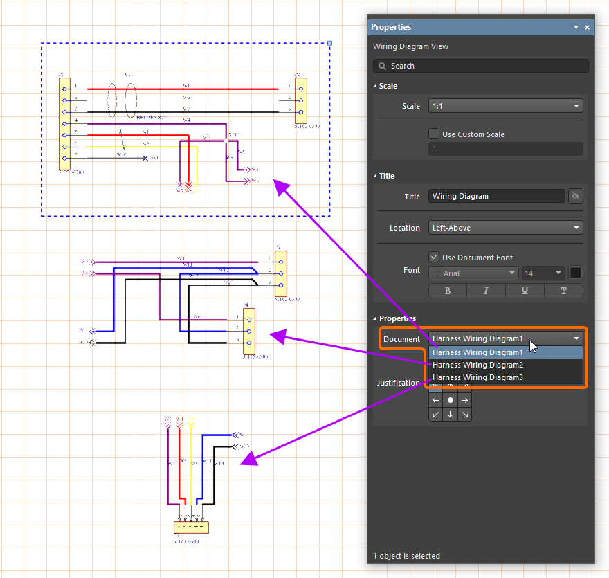
The Harness Draftsman document (*.HarDwf) now supports multiple Wiring Diagram documents (*.WirDoc) in the same project. This feature lets you choose the wiring diagram document from which a placed wiring diagram view should be generated and updated. Use the Document drop-down in the Properties region of the Properties panel when the wiring diagram view is selected to choose the wiring diagram document for this view.
Added Bookmarks Panel for Harness Draftsman Documents
The Bookmarks panel is now available in Draftsman when working with a manufacturing drawing of a harness design (*.HarDwf). The panel gives a tree view of the sheets on the Draftsman document. Each sheet entry can be expanded and collapsed. When expanded, the appropriate contents of each sheet are displayed as shown in the image below.
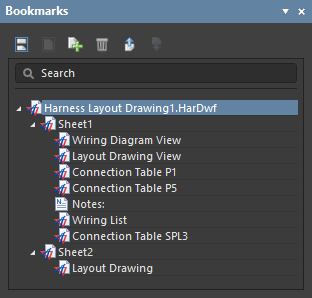
You can use the panel to easily navigate in the design space. When an item is selected in the panel or design space, the Properties panel (if open) displays the properties and settings of the selected item. Additionally, when you select an item in the Bookmarks panel, the design space zooms to the selected item.
Data Management Improvements
SiliconExpert Enhancements
Added SiliconExpert Product Change Notice
The Product Change Notice (PCN) provided by SiliconExpert has been added to the Manufacturer Part Search panel and to all places where part choices can be accessed. By default, the latest PCN data is shown. Use the Historical Details control to open the Product Change Notice Historical Details dialog, where details on previous PCNs can be browsed.
❯ ❮
Javascript ID: SE_PCN
|
Access the latest and historical PCNs from the Manufacturer Part Search panel.
Access the latest and historical PCNs from a part choice (the Components panel is shown as an example here).
|
Added SiliconExpert 'Free' Parameters Support
The Lifecycle, YTEOL and RoHS Status parameters provided by SiliconExpert are now presented by default in the Manufacturer Part Search panel and all places where part choices are presented. Therefore, there is no need to request data for this part (and hence, use the quota from your SiliconExpert package) to access these 'free' parameters.
❯ ❮
Javascript ID: FreeSEParameters_AD24_2
|
Access 'free' parameters provided by SiliconExpert from the Manufacturer Part Search panel.
Access 'free' parameters provided by SiliconExpert from a part choice (the Components panel is shown as an example here).
|
Also, these SiliconExpert 'free' parameters can be used in ActiveBOM (by adding corresponding columns to the ActiveBOM document) without requesting all other SiliconExpert parameters.
Added Display of the YTEOL Parameter
The YTEOL parameter is now displayed in the following locations:
- In the header of the Details pane when a manufacturer part is selected in the Manufacturer Part Search panel.
- In the header of the Details pane when a component is selected in the Components panel.
- In all places where part choices are presented.
- In the Properties panel when a component placed on a schematic sheet is selected.
❯ ❮
Javascript ID: SE_YTEOL_AD24_2
|
Displaying the YTEOL parameter in the Manufacturer Part Search panel.
Displaying the YTEOL parameter in the Components panel and in part choices.
Displaying the YTEOL parameter in the Properties panel for the selected component.
|
Added Support for SiliconExpert Parameters when Comparing Manufacturer Parts
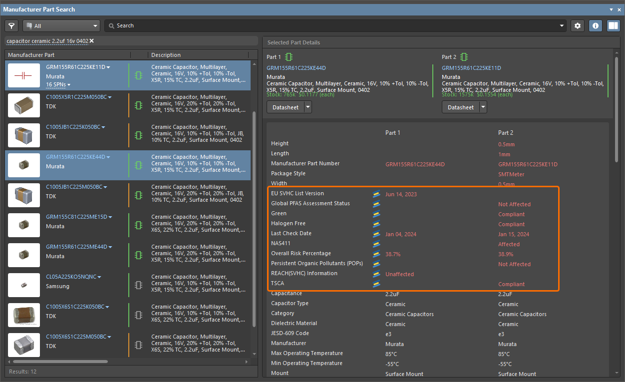
SiliconExpert parameters are now supported in the Selected Part Details pane of the Manufacturer Part Search panel when comparing two selected parts.
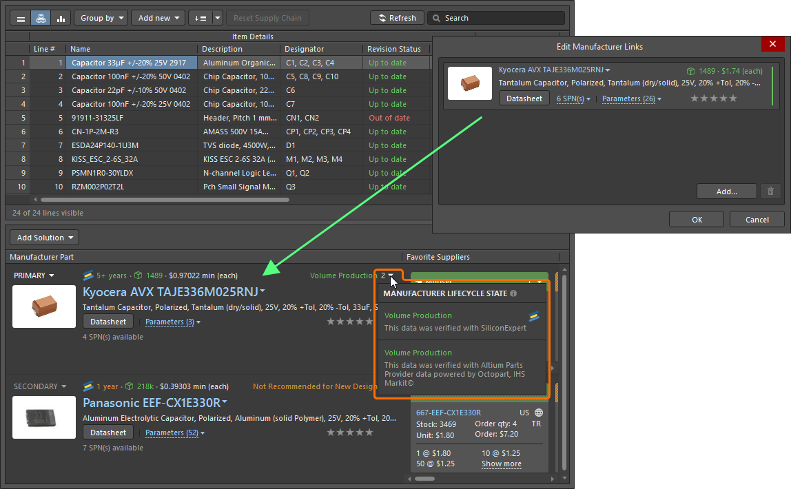
Added Support for Aggregated Lifecycles to Manufacturer Links
When exploring a solution added in the form of a manufacturer link to an ActiveBOM document if there are multiple sources of the lifecycle data for that manufacturer link (Altium Parts Provider powered by Octopart or IHS Markit® and SiliconExpert), the lifecycle information from all available sources is now accessible for the link. Hover the cursor over the manufacturer lifecycle state or use the drop-down to see the lifecycle information from all sources in the tooltip/pop-up.
Import/Export Improvement
Importing the Footprints into Existing Project Structure for Xpedition
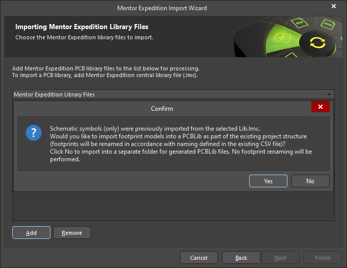
For an Xpedition library (*.lmc) whose schematic symbols (only) were previously imported using the xDX Designer Import Wizard with the Import Symbols Only option enabled, you can now choose to import footprint models into a PCBLib as part of the existing project structure. Footprints will be renamed in accordance with the naming defined in the existing CSV file generated as part of the xDX Designer import process.
Note that starting from this release, footprint names with specific prefixes (BGA, CAP, CAPC, CGA, COUP, DFN, DIO, DR, FILT, FUSE, INDC, INDM, ISOL, LEDC, LEDS, LGA, MECM, OSC, PQ, PS, QFN, QFP, RESC, RESM, SO, TO, VAR, XTA) will include the component height values multiplied by 100 in the generated CSV files to provide unique naming of footprints with differing 3D Body heights. For example, a footprint of height 1.4 and named CAPC2013N will be added to the CSV file as CAPC2013X140N.
When adding an Xpedition library file on the Importing Mentor Expedition Library Files page of the Import Wizard, if previously imported libraries are detected, a confirmation dialog will ask if you would like to import footprints as described above. If you click No, footprints will be imported into a separate folder for generated PCBLib files, and no footprint renaming will be performed.
Feature Made Fully Public in Altium Designer 24.2
The following feature is now officially Public with this release:
Altium Designer 24.1
Released: 16 January 2024 – Version 24.1.2 (build 44)
Release Notes for Altium Designer 24.1.2
Key HighlightsExpandСвернуть
Schematic Capture Improvement
Added Violation Checks for Objects Connected to a Harness Connector
In this release, new violation checks have been added to detect violations associated with signal harnesses in the schematics of your PCB design projects:
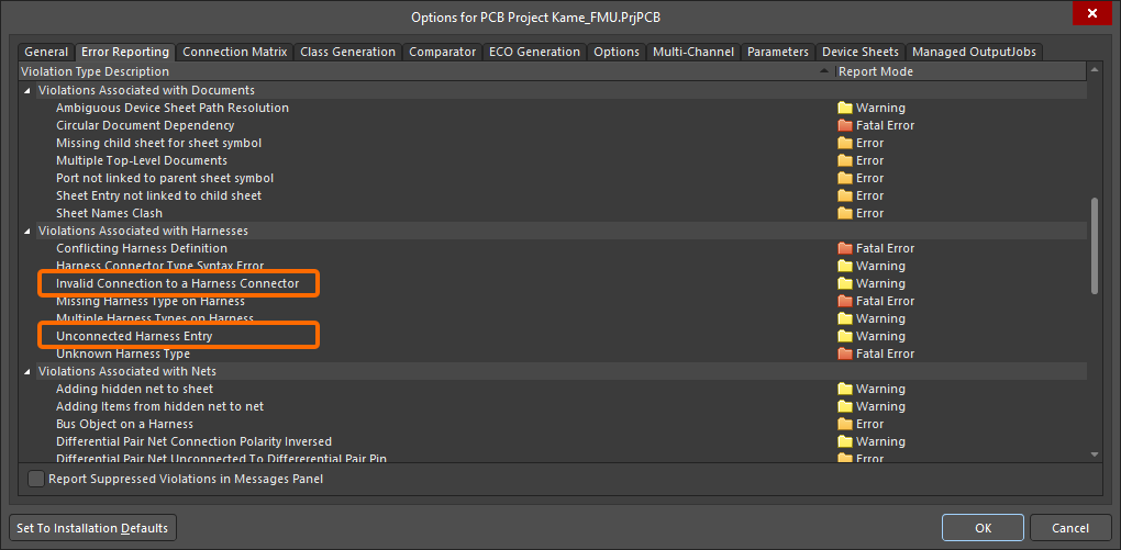
- The Invalid Connection to a Harness Connector violation check detects a situation when a wire, bus, or signal harness ends inside or is connected to the edge of a harness connector but is not connected to a harness entry.
- The Unconnected Harness Entry violation check detects an unconnected harness entry.
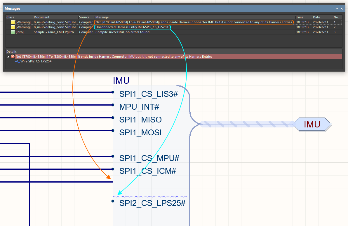
Settings for these violation types can be found in the Violation Associated with Harnesses group on the Error Reporting tab of the Project Options dialog.
PCB Design Improvements
Pad Hole Clearance Check Improvement (Open Beta)
In this release, the behavior of detecting clearance from pads with no annular ring has been improved.
When a pad has a hole size greater than or equal to the pad size and, therefore, has no annular ring, the clearance value defined for the Hole by the applicable constraint in the Constraint Manager or by the Clearance design rule is applied rather than the maximum of Hole and TH Pad clearances.
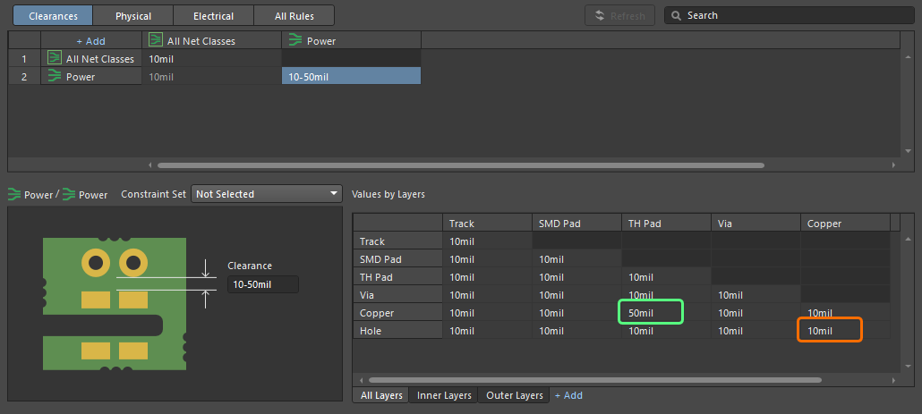
An example of clearances configured in the Constraint Manager.
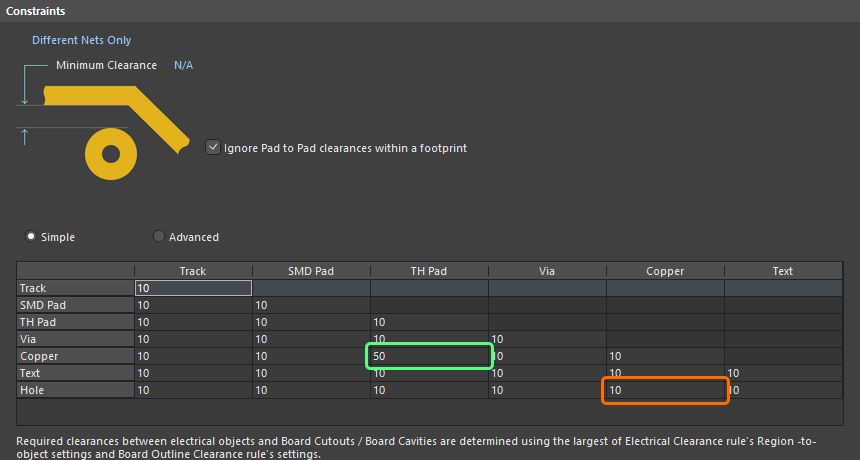
An example of clearances configured in the Clearance design rule.
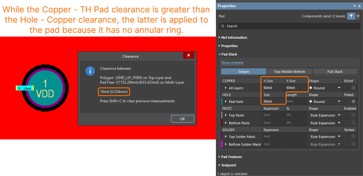
The new pad hole clearance behavior.
Note that the default values of Hole clearance in newly created Clearance constraints and Clearance design rules have been updated with the 10mil / 0.254mm value.
This feature is in Open Beta and available when the
PCB.Rules.HoleClearance option is enabled in the
Advanced Settings dialog.
Ability to Store TrueType Fonts (Open Beta)
This release has added the ability to automatically store geometries of text objects that use TrueType fonts inside PCB documents. When objects (text strings/frames, dimensions, drill tables, and/or layer stack tables) in a PCB document use a TrueType font, these objects will be shown using the same font geometry when the PCB document is opened on another computer, even if that TrueType font is not installed.
When an object that uses a missing font is selected, a warning message appears at the top of the Properties panel. When changing object properties that affect its text (e.g., the text height or text itself), the Missing fonts dialog opens in which you can select a replacement font.
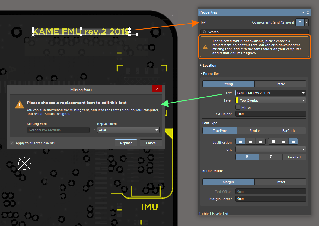
The dialog also appears when changing text-related properties from the PCB List panel.
When trying to edit multiple objects using different missing fonts, the dialog allows you to select a replacement for each missing font.
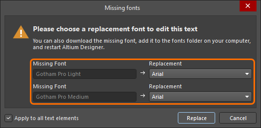
This feature is in Open Beta and available when the PCB.Text.TTFontSaving option is enabled in the Advanced Settings dialog.
Note that with this feature enabled, the options of the PCB Editor – True Type Fonts page of the Preferences dialog are no longer relevant, so this page is not available in the Preferences dialog (when the PCB.Text.TTFontSetting.Hide option is enabled in the Advanced Settings dialog).
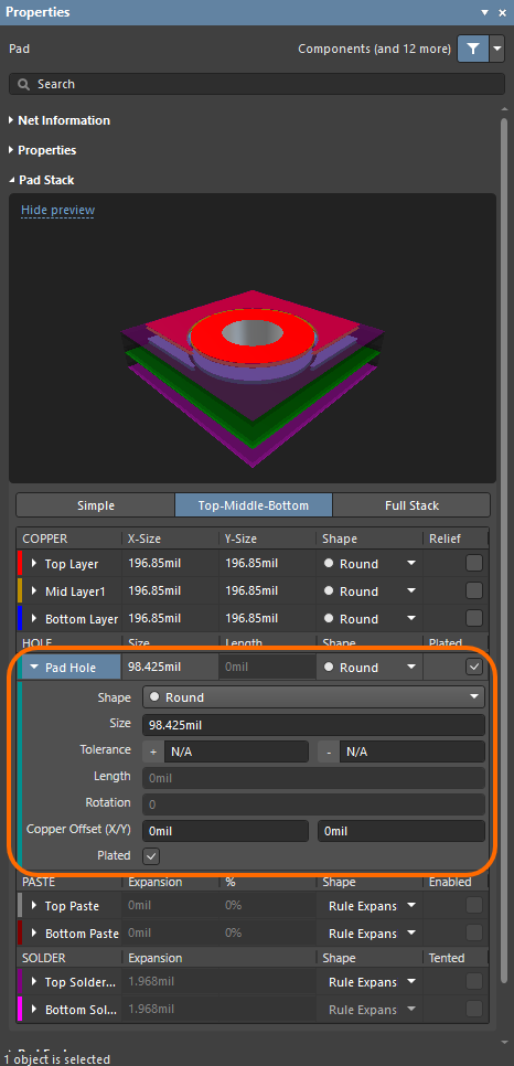
Enhanced Pad Properties Panel
The Pad Stack region of the Pad Properties panel has been enhanced for better usability. When a section is selected, the section name is highlighted in blue and the entire section is displayed in a different shade than the background.
PCB CoDesign Improvements
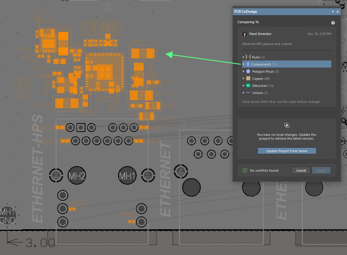
Ability to Highlight Category Changes
With the Show on PCB option enabled in the PCB CoDesign panel, you can now highlight all changes in a specific category when that category is selected in the panel's list of changes.
Grouping Changes by Unions
Added support for comparison of, and application of changes to, unions (defined groupings of primitives on the PCB). Union-related changes are shown in the Unions category in the PCB CoDesign panel's list of changes. Also, changes in other categories are grouped now by unions if corresponding objects belong to any.
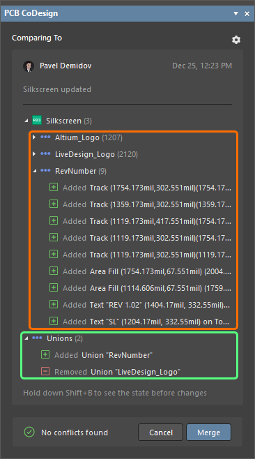
Updates to 'Merged' State
After merging changes using the PCB CoDesign panel, the PCB document will remain in the Merged state (the  icon in the Projects panel) until there is a new conflict. Saving changes locally will no longer change the state to Modified.
Also, note that documents in Merged state are always enabled for saving to the Workspace in the Save to Server dialog and cannot be disabled.
Constraint Manager Improvements
Ability to Choose Usage of the Constraint Manager for a New Project
When creating a new PCB project, you now have the ability to control whether it will use the Constraint Manager or the older design rules system. In the Create Project dialog (File » New » Project), enable the Constraint Management option to use the Constraint Manager for the project being created.
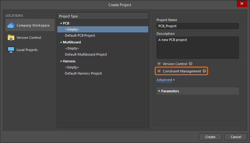
'View Only' Mode
If the Constraint Manager was enabled for the PCB project, the Constraint Manager will present in View Only mode when opened by a user without Altium Designer Pro/Enterprise Subscription. In this case, the user can see, but not modify, defined constraints. The message at the top of the Constraint Manager notifies you when the Constraint Manager is in View Only mode.

Updates to xSignal Creation
This release sees some updates in defining xSignals using the Constraint Manager:
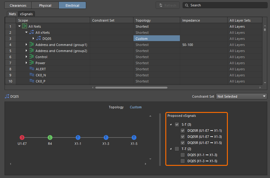
- The list of proposed xSignals is now divided into two groups: xSignals going from a source to a destination point (S-T) and xSignals going from one destination point to another (T-T). Use checkboxes for groups to select/deselect all xSignals in corresponding groups.
- The list of proposed xSignals now includes xSignals going from a source to each destination (not an xSignal going from a source to the closest destination only).
-
For a better representation of proposed xSignals, they are now named in the list using the following scheme:
<SourceNetName> (<SourcePinDesignator> → <DestinationPinDesignator>)
Note that for names of created xSignals that can be seen on the xSignals tab to the Constraint Manager or in the PCB document, the previous <SourceNetName>_<SourcePinDesignator>_<DestinationPinDesignator> scheme is used.
Improved Class Selection
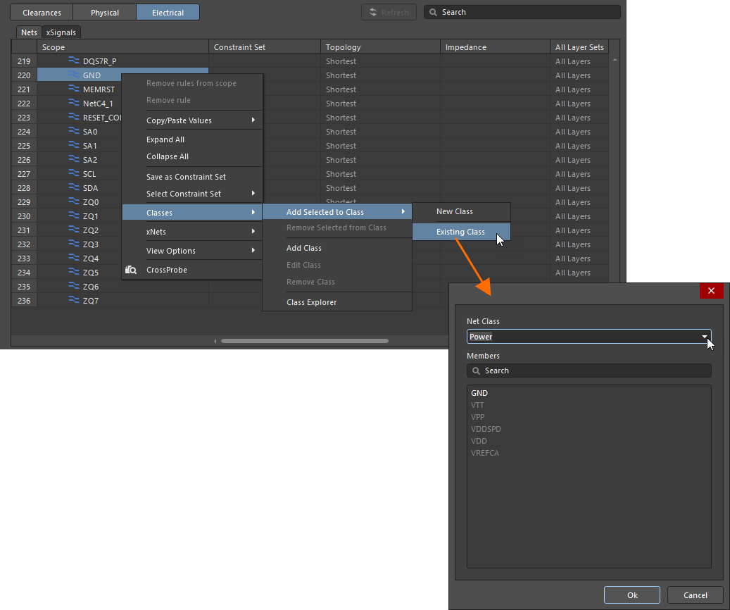
The right-click menu of entries in the Physical and Electrical views has been updated to quickly add objects to an existing class right from the menu. To do this, right-click one or more selected objects and choose an existing class from the Classes » Add Selected to Class sub-menu.
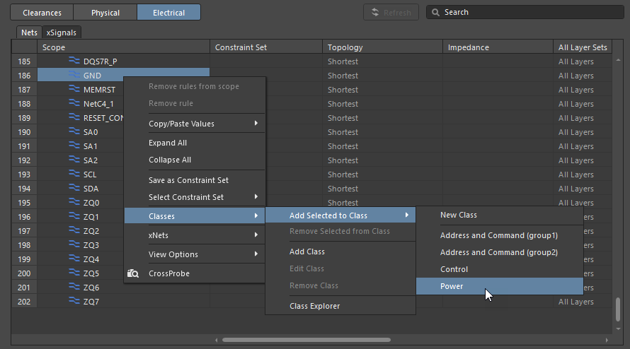
When there are more than 30 classes, the Classes » Add Selected to Class » Existing Class command is available in the menu instead of the list of classes. Use this command to access a dialog where you can select an existing class to which the selected object(s) are to be added.
Added Line Numbers in Grid
Line numbers have been added to the Constraint Manager grid to help you more easily identify and distinguish items in the list.

Multi-board Design Improvements
Support for Draftsman Documents in Multi-board Projects (Open Beta)
You can now add a Draftsman document (*.MbDwf) to a Multi-board project to create a manufacturing drawing for the Multi-board assembly in this project.
The views that can be placed in a Draftsman document of a Multi-board project are:
- Multi-board view – an automated graphic composite of the outlines of PCBs and 3D models constituting the multi-board assembly.
- Section view – a profile slice, or sectional, drawing taken from a nominated 'cut' point through a placed multi-board view.
- Board detail view – a floating, magnified view of a multi-board view's defined area.
- Board realistic view – a scalable 3D rendering of the current multi-board assembly.
Draftsman's annotation, dimensioning and graphical tools, as well as BOM and generic tables, are also available.
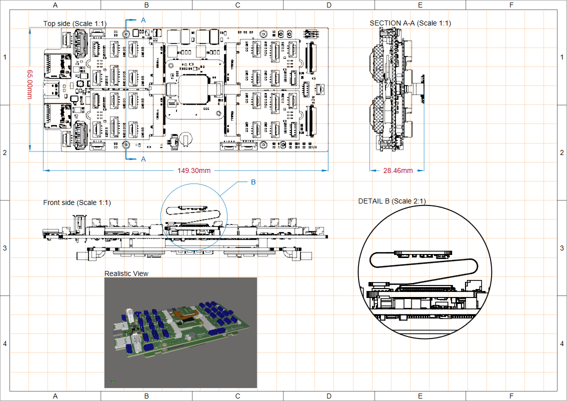
An example of a Multi-board project Draftsman drawing.
Ability to Move a Module Entry Group
The ability to move a selected group of module entries in a multi-board schematic document (*.MbsDoc) has been added. This new feature speeds up the editing process by not requiring you to move each module entry individually. In the design space, select more than one module entry, then use the left mouse button to drag the group to the desired location. A red dot displays at each entry while they are dragged to the new location. Release the mouse button to place the group at the current location.
Harness Design Improvements
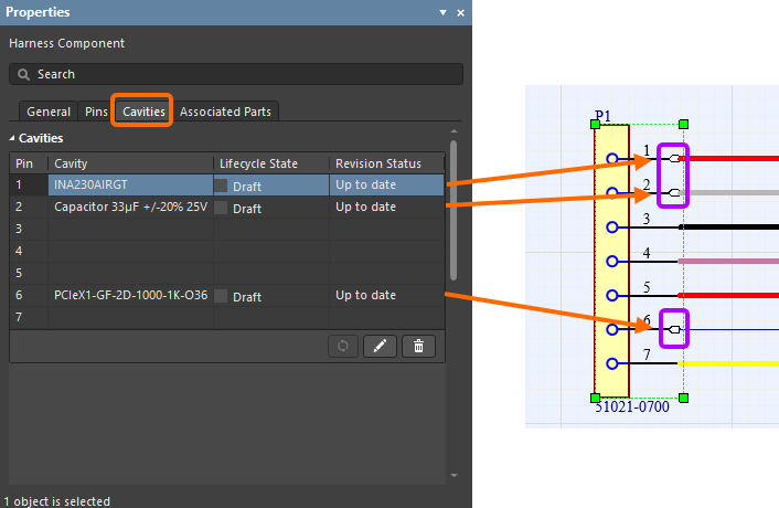
Changed 'Crimps' to 'Cavities'
'Crimps' have been renamed 'Cavities' in the UI of the Wiring Diagram and Layout Drawing.
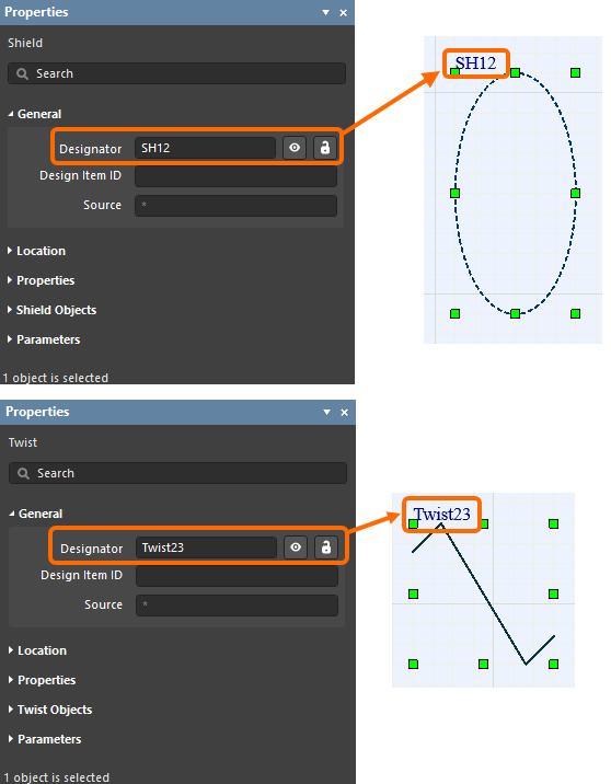
Added Designator Field to Shield and Twist Objects
The Designator field has been added to the properties of shields and twists in the harness wiring diagram.
Added Wire Break Object for Multiple Sheet Capability
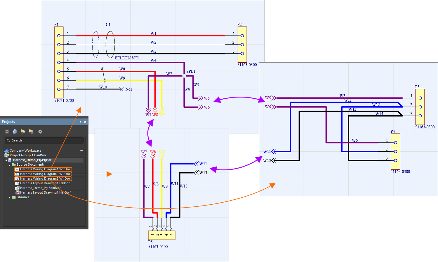
A full Wiring Diagram can now be defined over multiple sheets (in a 'flat' design fashion), each represented by its own *.WirDoc document, with the ability to split a wire using the new Wire Break object.
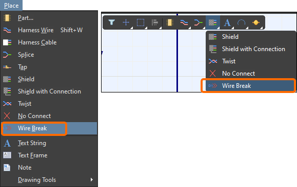
A Wire Break is placed using the Place menu or from the Active Bar as shown below.
Treat Coverings as Components in BOM
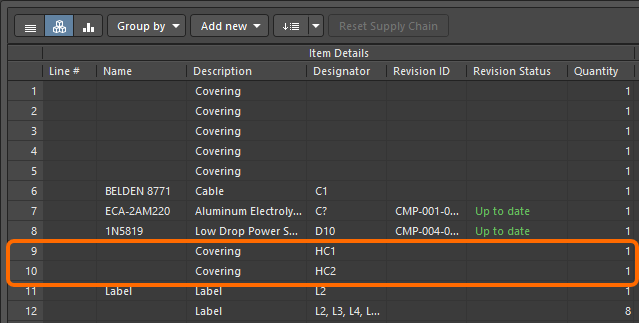
Harness coverings in the Layout Drawing are now treated as components in the BOM, with support for part choices and grouping.
Display Component Properties for Additional Physical Views
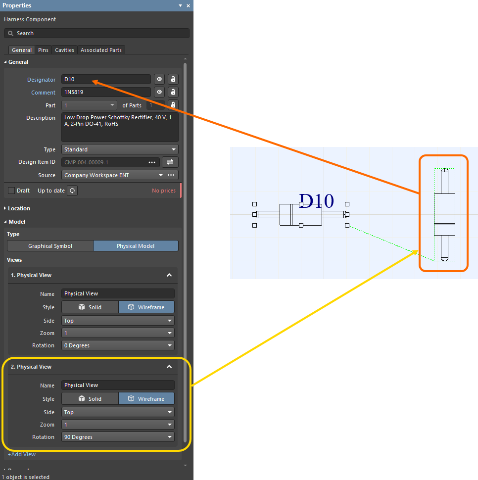
When an additional physical view of a harness component is selected in the design space, the Properties panel now displays the properties of the component itself as it does for the main (first) physical view. In the below image, a second physical view has been selected in the design space; the Harness Component Properties panel displays the properties of the original (first) physical view.
Improved the Wiring List
Added Ability to 'Split' Wiring List
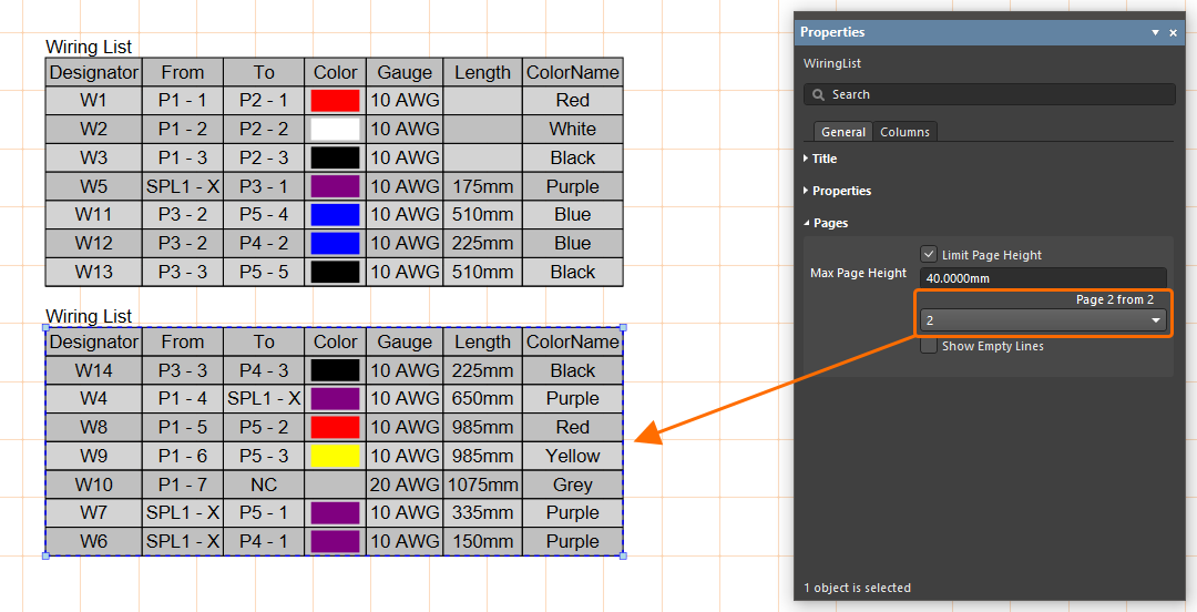
The wiring list of an advanced harness design may have a large number of entries, which can be difficult to fit into a drawing document as a single table. Rather than resorting to font and table scaling, multiple custom table entries, or an external document, you now have the ability to 'split' a Wiring List in a Harness Draftsman document so that the Wiring List will be presented over a number of 'pages.' In the Properties panel for a placed Wiring List, enable the Limit Page Height option in the Pages region to use the new feature. This will restrict the height of the Wiring List table to the nominated height entry (Max Page Height) and, therefore, the number of lines shown in the table.
❯ ❮
Javascript ID: Harness_MD_WiringList_LimitPageHeight
|
The editor detects that the entire Wiring List is not shown, as indicated by the panel's Page entry (for example, 1 from 2), and the associated drop-down menu allows you to nominate which page is shown. To add further pages of the Wiring List, place another Wiring List (Place » Wiring List) and specify the next Page in the Pages region of the Properties panel.
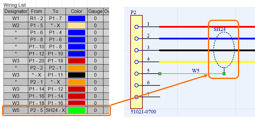
Enhanced Wiring List for 'Shield with Connection' Objects
Designators of shield with connector objects are now displayed in the Wiring List when a wire is connected to the shield's connector.
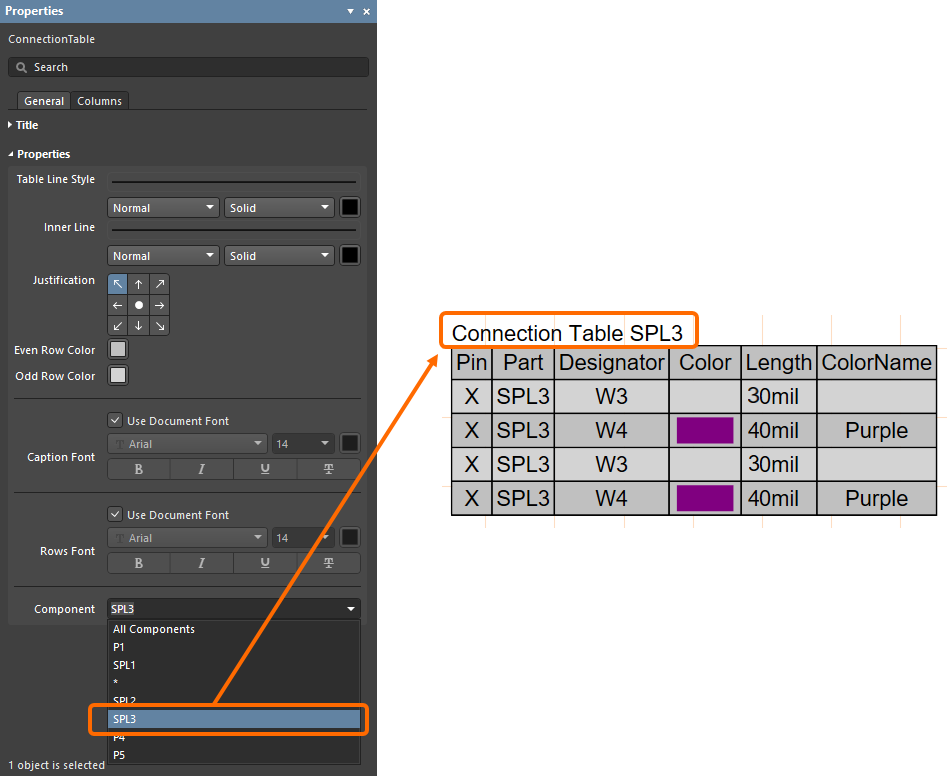
Added Ability to Display Connection Table for Splices
The ability to show the connection table for individual splices has been added. Previously, the ability to show the Connection Table for only components and connectors was possible.
Links Added to Text Frame and Note Objects for Cross-Probing
Object designators can now be added as active links in text frames and notes. The links provide cross-probe capabilities in the Wiring Diagram and Layout Drawing. To create active links, place a text frame or note object in either the Wiring Diagram or Layout Drawing. In the Text field in the Properties region of the Properties panel, enter "@". A drop-down of all designators will appear. Double-click the desired designator from the li st; the link is created in the Text field and in the design space. Click the link in the design space to cross-probe to that object in the associated document (i.e., the document that is not currently active). The process is demonstrated in the video below.
Data Management Improvements
Manufacturer Lifecycle State Message Enhancement
When using the SiliconExpert integration functionality, manufacturer part lifecycle data can be obtained from different sources: Altium Parts Provider (powered by Octopart or IHS Markit®) and SiliconExpert. To provide better visibility of this lifecycle data from different sources, the lifecycle information from all available sources is now accessible.
When exploring manufacturer part data (e.g., an entry in the Manufacturer Part Search panel, a part choice of a Workspace library component, or a solution in an AcitveBOM document), hover the cursor over the manufacturer lifecycle state/bar or use the drop-down to see the lifecycle information from all sources in the tooltip.
❯ ❮
Javascript ID: ManufacturerLifecycle_MultipleSources_AD24_1
|
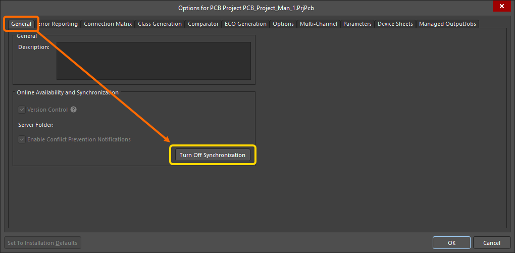
Added General Tab to Project Options for Offline Workspace Projects
Added the General tab to the Project Options dialog for offline Workspace projects. This feature is available for working with a project when you are disconnected from its Workspace. The only control on the tab that is accessible is the Turn Off Synchronization button. Click this button to turn off synchr onization. This ensures that the local copy will not be linked to the one that resides on the Workspace. The project located in the Workspace will remain untouched.
Removed Commit Command for Git-based Projects
For Git-based projects, the Commit command has been removed from the History & Version Control sub-menu of the right-click menu of project entry in the Projects panel and the Project main menu, aiming to remove confusion about where data was being committed (to the local repository and not the remote repository) when using the command. Visibility of the command is controlled by the VCS.AllowGitCommit option from the Advanced Settings dialog (OFF by default). You can use the Save to Server command to commit the project to the local repository and push it to the remote repository in one action.
Import/Export Improvement
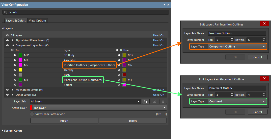
Mentor Xpedition Placement Outline and Insertion Ouline Layer Mapping
When Mentor Xpedition PCB and footprint library files are imported, Placement Outline layer types are now mapped as Courtyard layer types and the Insertion Outline layers are now mapped to the Component Outline layer types in Altium Designer.
Circuit Simulation Improvement
Simulation Stress Analysis (Open Beta)
Stress Analysis is used to calculate operating conditions for each individual component, such as maximum voltages, currents, and power dissipations, and check them against limits defined in the stress model of the component.
In this release, a new Stress Analysis option has been added to the Transient region of the Simulation Dashboard. When this option is enabled and the Transient analysis is performed, the Stress analysis results are available on the additional Stress chart of the simulation result document.
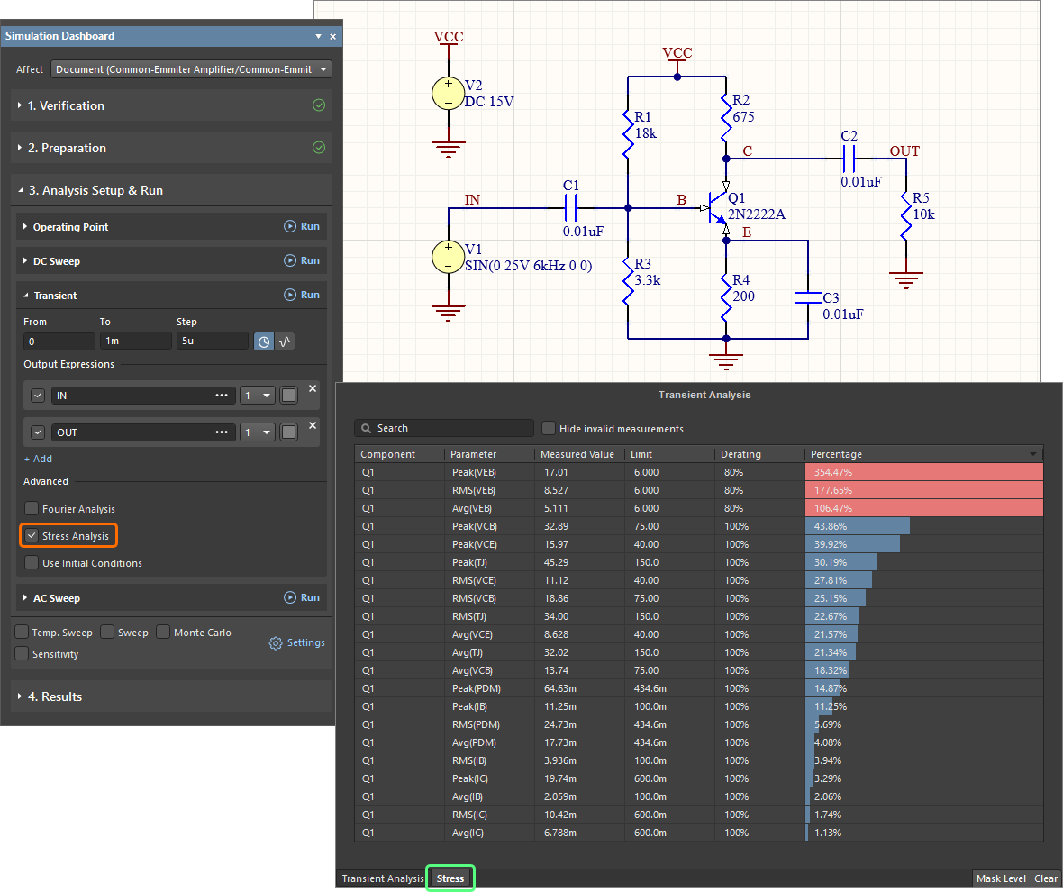
Use the new Stress Analysis to test your circuits against defined limits.
The stress model of a component is configured on the new Stress tab of the Sim Model dialog accessed for the component's simulation model. From here, you can select the required Device Type and define parameter values.
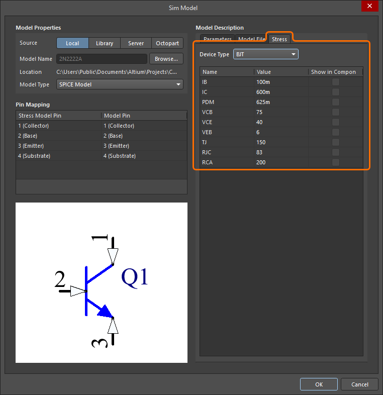
Stress analysis parameters for a component can be set on the Stress tab of the Sim Model dialog.
This feature is in Open Beta and available when the
Simulation.StressAnalysis option is enabled in the
Advanced Settings dialog.
Feature Made Fully Public in Altium Designer 24.1
The following feature is now officially made Public with this release:
Altium Designer 24.0
Released: 13 December 2023 – Version 24.0.1 (build 36)
Release Notes for Altium Designer 24.0.1
Key HighlightsExpandСвернуть
PCB Design Improvements
Any Angle Diff Pair Router (Open Beta)
This release introduces support for any angle differential pair routing. When routing a diff pair using the Interactive Differential Pair Routing tool (Route » Interactive Differential Pair Routing), you can now select the Any Angle corner style ( ) when configuring the properties of routing in the Properties panel in its Differential Pair Routing mode.
- Any angle differential pair routing supports symmetrical pad entry and gap changing.
- When starting differential pair routing from an antenna, the tool will maintain the left-to-right order of nets (i.e., the continuation of the left side stays on the left) and support snapping to the original direction.
- When routing a diff pair using the Any Angle corner style, press and hold the Shift key to route the diff pair using tangent arcs.
Demonstration of any angle differential pair routing.
Note that this feature also enables an updated angle diff pair glossing algorithm when using the Route » Gloss Selected command.
The current main limitations of any angle diff pair routing are:
- Routing transitions through borders of rooms with different design rules are not currently supported.
- The SMD Entry design rule is not currently supported.
- Automatic loop removal is not currently supported.
This feature is in Open Beta and is available when the
PCB.Routing.AnyAngleDiffPairRouter option is enabled in the
Advanced Settings dialog.
Enhanced Layer Stack Report Setup Dialog (Open Beta)
The Layer Stack Report Setup dialog (File » Fabrication Outputs » Report Board Stack) has been enhanced and now includes all columns that are present in the Layer Stack. Use the dialog to select the columns you want to be displayed in the Layer Stack Report.
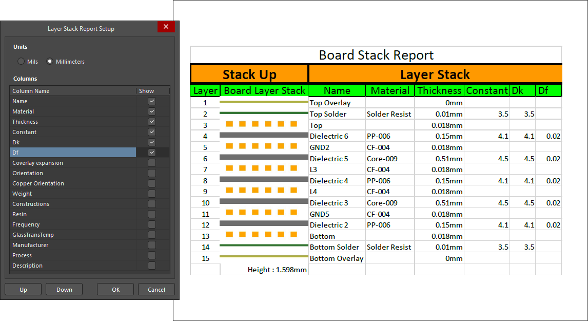
This feature is in Open Beta and available when the
PCB.ModernBoardStackGenerator option is enabled in the
Advanced Settings dialog.
PCB CoDesign Improvements
Enhanced Copper Conflict Display and Resolution
Conflicts of copper objects are now grouped in pin-to-pin connection groups where applicable to ease exploring and resolving the changes.
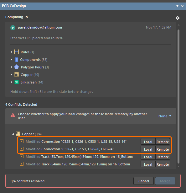
Copper conflicts can now be resolved on the pin-to-pin connection level.
Added Ability to Configure Color Legend
In the View Configuration panel, you can now select colors for objects that have been added, modified, removed, and not changed (unchanged objects of a pin-to-pin connection when it is selected in the PCB CoDesign panel).
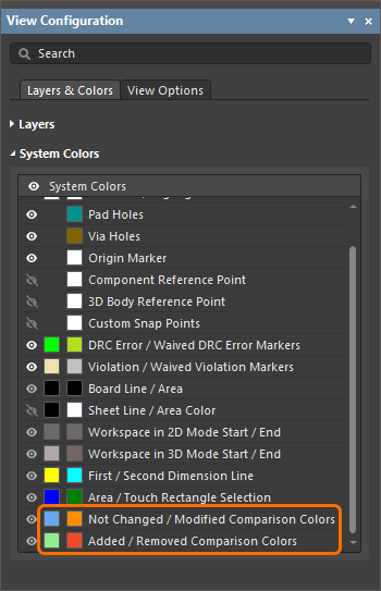
Use the View Configuration panel to configure the comparison color legend.
Other PCB CoDesign UI Changes
- The pop-up that shows that the comparison is in progress now appears right after running the comparison.
- Added the ability to select and deselect entries in the change list. When an entry is selected (by clicking on it), click it again to deselect the entry and reset the object highlighting in the design space.
- The Save to Server command has been added to the menu of the Project panel's Merged icon (
 ) shown after merging changes using the PCB CoDesign panel –
 ![]() show image.
show image.
- When clicking the Save to Server button in the PCB CoDesigner panel after merging changes, only the merged PCB document is selected in the Save to Server dialog by default –
![]() show image.
show image.
- When merging the changes is run, a new pop-up showing that merging is in progress is now displayed –
![]() show image.
show image.
Constraint Manager Improvements
Ability to Add Differential Pair Classes to the Clearance Matrix
Starting from this release, you can add not only net classes but also differential pair classes to the Clearance Matrix (the Clearances view).

Editing Custom Topology on the PCB Side
It is now possible to define the topology of a net as Custom and edit it as required in the Constraint Manager when it is accessed from the PCB side.
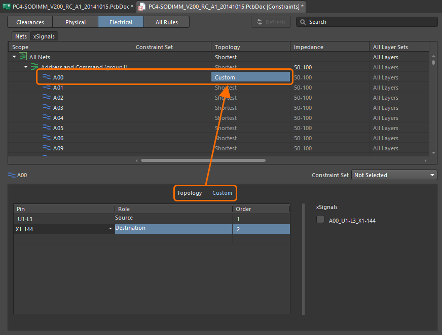
Propagating Topology Changes when Editing the Constraint Set
When editing a Constraint Set that includes a custom topology, changes made to the topology are now propagated to other objects to which this Constraint Set is applied.
Ability to Remove xSignals
It is now possible to remove an xSignal from the xSignals tab of the Electrical view. To do this, right-click an xSignal and select the xSignals » Remove xSignal command from the context menu.
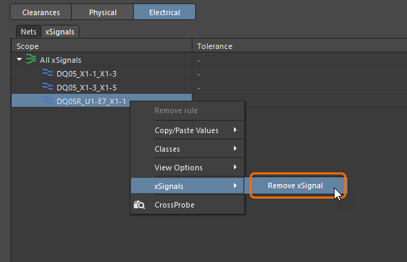
Cross Select From and To the Constraint Manager
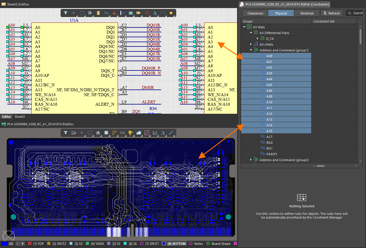
In this release, an ability to cross-select objects from and to the Constraint Manager has been added. When cross-select mode is enabled (using the Cross Select Mode command from the Tools main menu of the Constraint Manager, the schematic or PCB editor), objects selected in the Constraint Manager are also selected in the schematic and PCB documents, and vice versa.
Enhanced the Expand/Collapse State
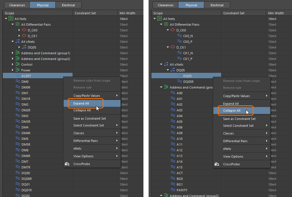
All nodes, except for those that are predefined (e.g., All Nets), are now collapsed in the Physical and Electrical views by default. You can use the new Expand All and Collapse All right-click menu commands to control the grid nodes.
3D-MID Design (Open Beta)
3D-MID technology combines electrical circuits with three-dimensional mechanical parts. This fusion of functionality opens up a world of possibilities within a vast range of application areas.
Historically, designers of 3D-MIDs have generally been restricted to MCAD packages due to the lack of suitable ECAD tools. There are many problems inherent to this way of working, not least is the absence of any electrical intelligence to drive the circuit layout and the difficulties associated with projecting 2D manually drawn sketches onto 3D surfaces.
The new 3D-MID editor in Altium Designer allows you to place standard surface mount components onto a 3D shape in a 3D-MID document and route traces along the surface of the shape to complete the layout.
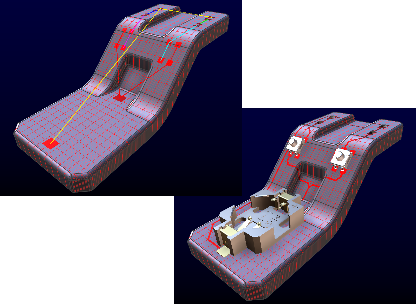
The completed design can then be exported in the file format required by the Laser Direct Structuring (LDS) manufacturing process.
Note that the 3D-MID functionality is not supported with the Altium Designer Standard Subscription. If you are interested in 3D-MID and have a Standard Subscription, talk to your Altium sales representative about your evaluation options.
Harness Design Improvements
Treat Layout Labels as Components in BOM
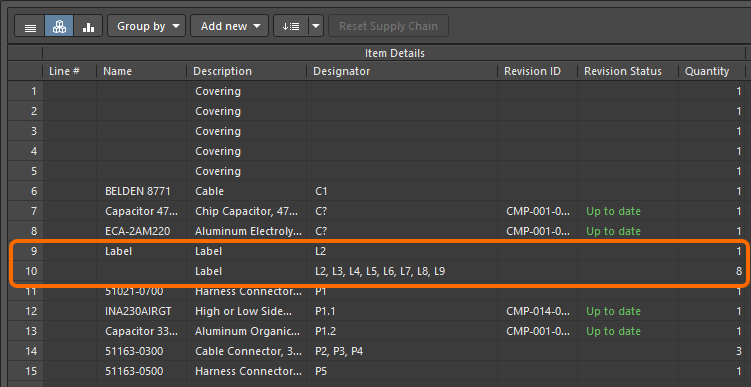
Layout labels in the Layout Drawing are now treated as components in the BOM, with support for part choices and grouping.
Added Columns to the Connection Table and Wiring List
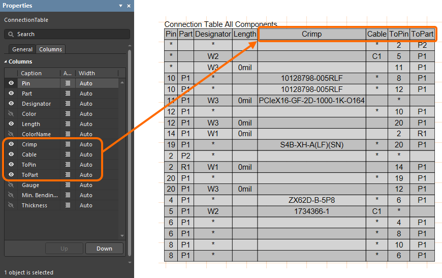
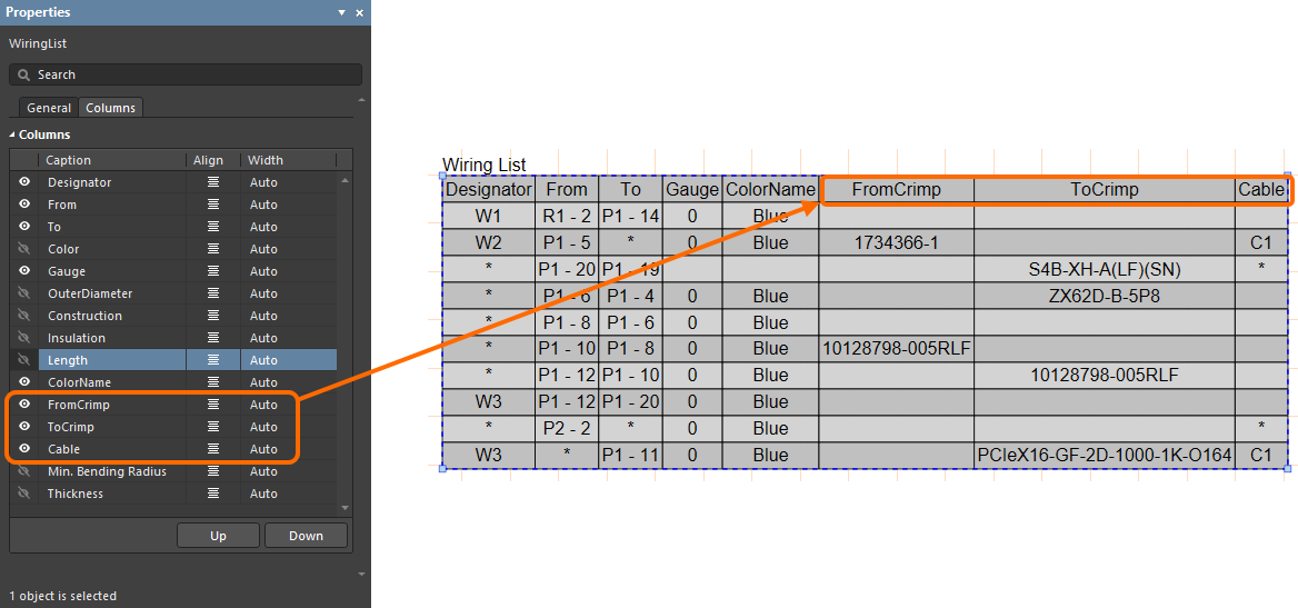
Additional columns have been added to the Connection Table and Wiring List in a Manufacturing Drawing (*.HarDwf) that allow you to easily view the additional information in the design space. Crimp (part number), Cable, ToPin, and ToPart have been added to the Connection Table; FromCrimp, ToCrimp, and Cable have been added to the Wiring List. Toggle the eye icon in the Properties panel to display/hide the desired columns in the connection table.
Platform Improvement
Support for Long Path Names (Open Beta)
Support for long path names has been implemented in this release. When a file path with the file name exceeds 256 characters, the actions on files are now supported, including:
- Opening a project from the connected Workspace.
- Making a local project available in the Workspace.
- Changing the folder path in an Outjob file.
- Generating outputs using an Outjob file or the Project Releaser.
- Saving a project as a project template to the Workspace.
Starting from Windows 10 version 1607, MAX_PATH limitations have been removed from common Win32 files and directory functions. However, you must opt-in to the new behavior by changing a registry key on the computer where Altium Designer is installed. Refer to the Support for Long Path Names page for details. After doing so, ensure that your computer is rebooted.
WARNING: Modifying the registry improperly can result in Windows becoming unusable. Use the Registry Editor only at your own risk and only after backing up the registry as outlined in the Microsoft article
How to back up and restore the registry in Windows.
When releasing a project that uses a long path to an Enterprise Server Workspace, the PC where the Altium On-Prem Enterprise Server is installed should also be configured:
learn more.
This feature is in Open Beta and is available when the
System.LongPathsSupport option is enabled in the
Advanced Settings dialog. Note that this option is available only when the
LongPathsEnabled registry key is set to
1.
Import/Export Improvements
xDX Designer Import Enhancements
This release delivers a number of key improvements and fixes in relation to the import of xDX Designer design files into Altium Designer.
Added Ability to Import Symbols Only
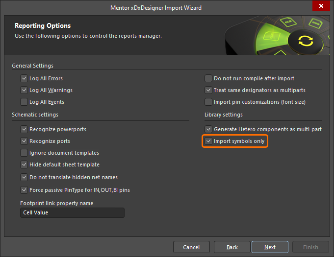
The Reporting Options page of the Mentor xDxDesigner Import Wizard now includes the Import symbols only option that allows to import symbols only. When this option is enabled, identical symbols from the library database will be imported as a single schematic symbol, even if it is used by many components in the original library, and parameters are not imported to symbols in Altium Designer.
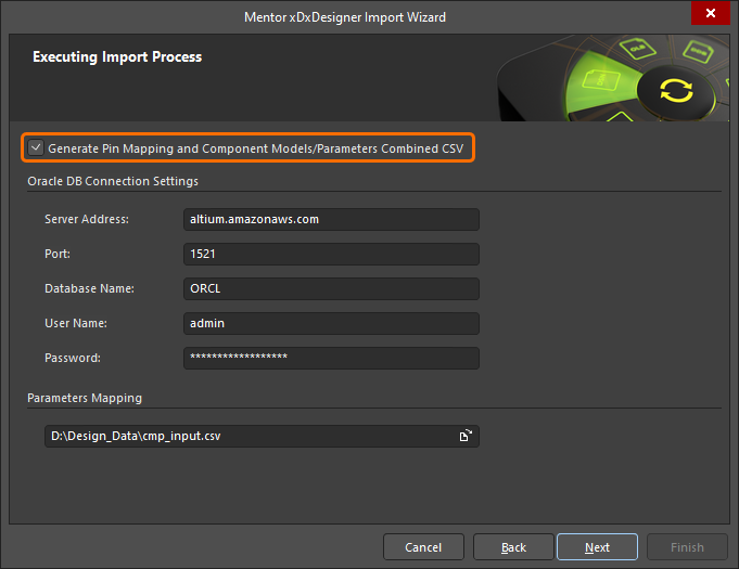
Also, when this option is enabled, the next page of the Wizard will suggest generating part-symbol and pin mapping data in CSV format by enabling the Generate Pin Mapping and Component Models/Parameters Combined CSV option. When this option is enabled, use the available fields to define Oracle DB connection parameters and a parameter mapping file.
Multi-part Symbol Import Improvements
When imported to Altium Designer, a multi-part symbol receives a Design Item ID combined with the first and last part names defined in xDX Designer. These combined Design Item IDs are also used in the generated CSV files.
Also, the order of parts in symbols imported to Altium Designer is now the same as defined in the original library.
Symbol Import Improvements
Other import improvements include:
Mentor Expedition Import Improvements
Added Ability to Choose Extruded Body Layer
You now have the ability to choose the layer when creating extruded bodies when importing Mentor Expedition files using the Import Wizard. After adding the Mentor PCB and Library files to be imported, choose from Placement Outline or Assembly Outline using the Create extruded body from drop-down on the Current User Layer Mappings page. When the option is enabled, the default is Placement Outline.
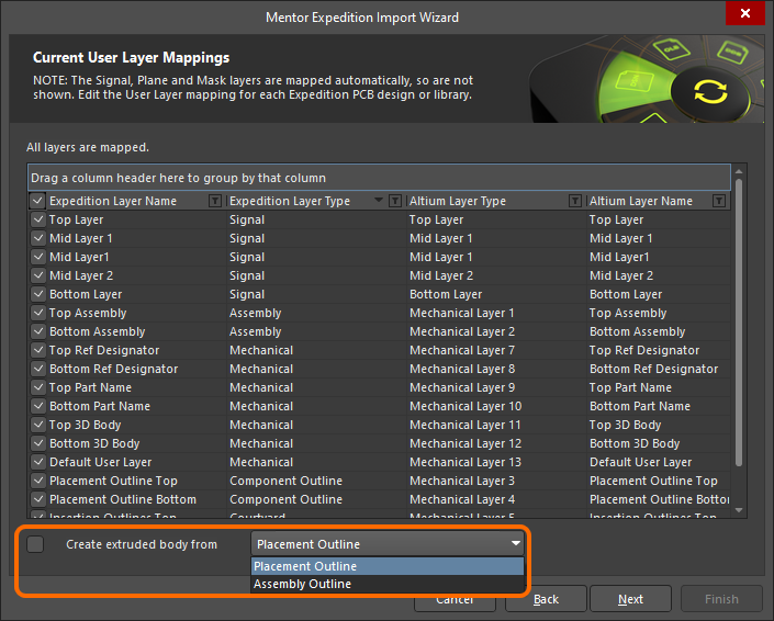
Placement Outline Improvement
Placement Outlines can now be imported as primitives on the Placement Outline layer on the Top/Bottom 3D Body assembly layers.
Circuit Simulation Improvement
Output Currents for P-Channel Transistors Inverted
Output currents for P-Channel transistors (BJT, JFET, MOSFET, MESFET) are now treated as inflow currents, making them consistent with N-Channel transistors.
Ansys CoDesigner (Open Beta)
This release presents the first steps into true collaborative design (CoDesign) between the ECAD and Simulation domains. Up until now, engineers in these two siloed camps have had to rely on manual export/import file processes that have no connection with a revision of a design and communication of changes and results, typically by email, outside of the design arena.
Now, with the arrival of the Ansys CoDesigner feature, the ECAD engineer (using Altium Designer) can seamlessly collaborate on a design with their SIM engineer colleague (using Ansys Electronics Desktop (AEDT)). Collaboration is facilitated through an Altium 365 Workspace, which acts as a bridge between the two domains. This initial release includes support for the following key elements:
- Bi-directional push/pull of design changes between the two domains. From Altium Designer, changes to layer stack and materials, components, and primitives are detected and can be applied in AEDT. From AEDT, proposed changes to layer stack and materials can be pushed through the EDB file and detected/applied in Altium Designer.
- Simulation results are pushed from AEDT to the Altium 365 Workspace and associated with a revision of the design, with the ability to view through the Workspace’s browser interface and preview within Altium Designer.
- Bi-directional communication using the commenting system, with each comment thread attached to a specific component in a design.
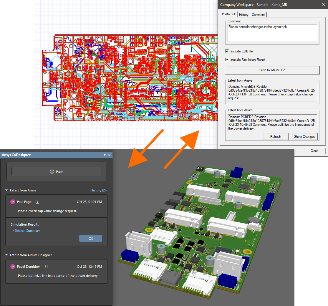
Currently, AEDT of version 2023 R1 and 2023 R2 is supported by Ansys CoDesigner.
Note that Ansys CoDesigner is not supported with the Altium Designer Standard Subscription.
This feature is in Open Beta and is available when the
Ansys CoDesigner (for Altium Designer) and
Altium Link (for Ansys Electronics Desktop) extensions are installed. The latter can be obtained by contacting
ansyscollaboration@altium.com.
Power Analyzer by Keysight Improvement
Added Ability to Assign Currents for Multiple Nets on the Same Component
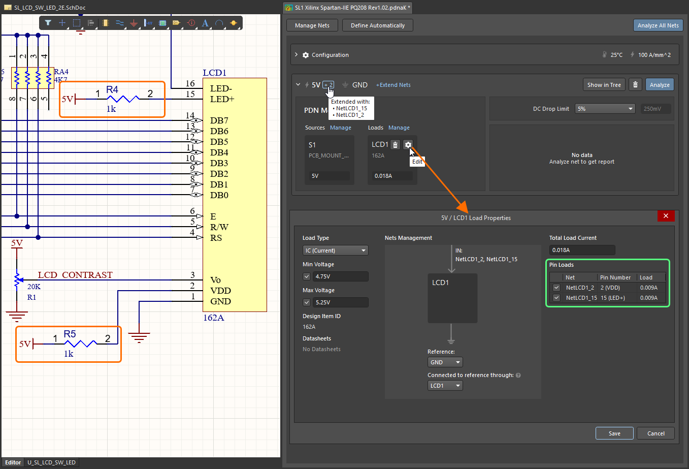
In this release, the ability to assign currents for multiple nets on the same component for different series elements has been added.
When configuring a load of the IC (Current) type, you can see all pins of the load component that connect it with the source through different serial components, with the ability to select the required pins.
In the example shown below, the 5V power net is connected to two pins of the LCD1 component through R4 and R5 series components. After extending the power net and adding LCD1 as the load, both pins can be selected and configured as required in the Load Properties dialog.
Features Made Fully Public in Altium Designer 24.0
The following features are now officially made Public with this release: