This page details the improvements included in the initial release of Altium Designer 23, as well as those added in subsequent updates. Along with delivering a range of improvements that develop and mature the existing technologies, each update also incorporates a large number of fixes and enhancements across the software based on feedback raised by customers through the AltiumLive Community's BugCrunch system, helping you continue to create cutting-edge electronics technology.
You can choose to continue with your current version, update your current version, or install Altium Designer 23 alongside your current version to access the latest features. Your current version can be updated from within the software in the
Extensions and Updates view. If you prefer to install Altium Designer 23 alongside your current version, visit the
Altium Downloads page to download the installer, then choose
New Installation on the
Installation Mode page of the installer.
Free Trial!
If you like what you see but are not yet a customer, why not take Altium Designer for a test drive? By filling out a simple form, you can try Altium Designer for free with 15 days of access to the full software. That's right, you will have the ability to evaluate the full Altium Designer experience with no technical limitations with unfettered access to the world's finest PCB design product. Click the link below, fill out the form, and see for yourself why more engineers and designers choose Altium than any other product available!
Altium Designer Free Trial.
Altium Designer 23.11
Released: 16 November 2023 – Version 23.11.1 (build 41)
Release Notes for Altium Designer Version 23.11
PCB Design Improvements
Replication of PCB Layout
This release includes the arrival of a new PCB Layout Replication tool that allows you to quickly replicate the layout for repetitive blocks of circuitry in a flat PCB design. You are no longer at the mercy of manual routines, nor do you have to touch snippets, reuse blocks, or convert your design into a multi-channel one.
As an informal reuse feature, this tool is a perfect fit when you need to quickly replicate the placement of a group of components to another group of the same, not-yet-placed components with the same connections.
On the PCB document, select a fragment of the captured design to be replicated (the Source Block), and then apply that layout to each fragment of the design that is detected to be a match (Target Blocks). You have full control over which target block(s) to apply replication to and can specify what that replication should include besides component placement (e.g., routing objects).
The video below demonstrates the process of using the tool.
This feature is in Open Beta and is available when the
PCB.LayoutReplication option is enabled in the
Advanced Settings dialog.
Automatic Tuning of Multiple Nets
This release brings automatic length/delay tuning (or multi-tuning) functionality to the PCB editor. Select the traces to be tuned, choose the Route » Automatic Length Tuning command from the main menus (shortcut Ctrl+Alt+T), configure the accordion-based pattern and its attributes as required in the Auto Tuning Process dialog, and the software will create the tuning patterns for you.
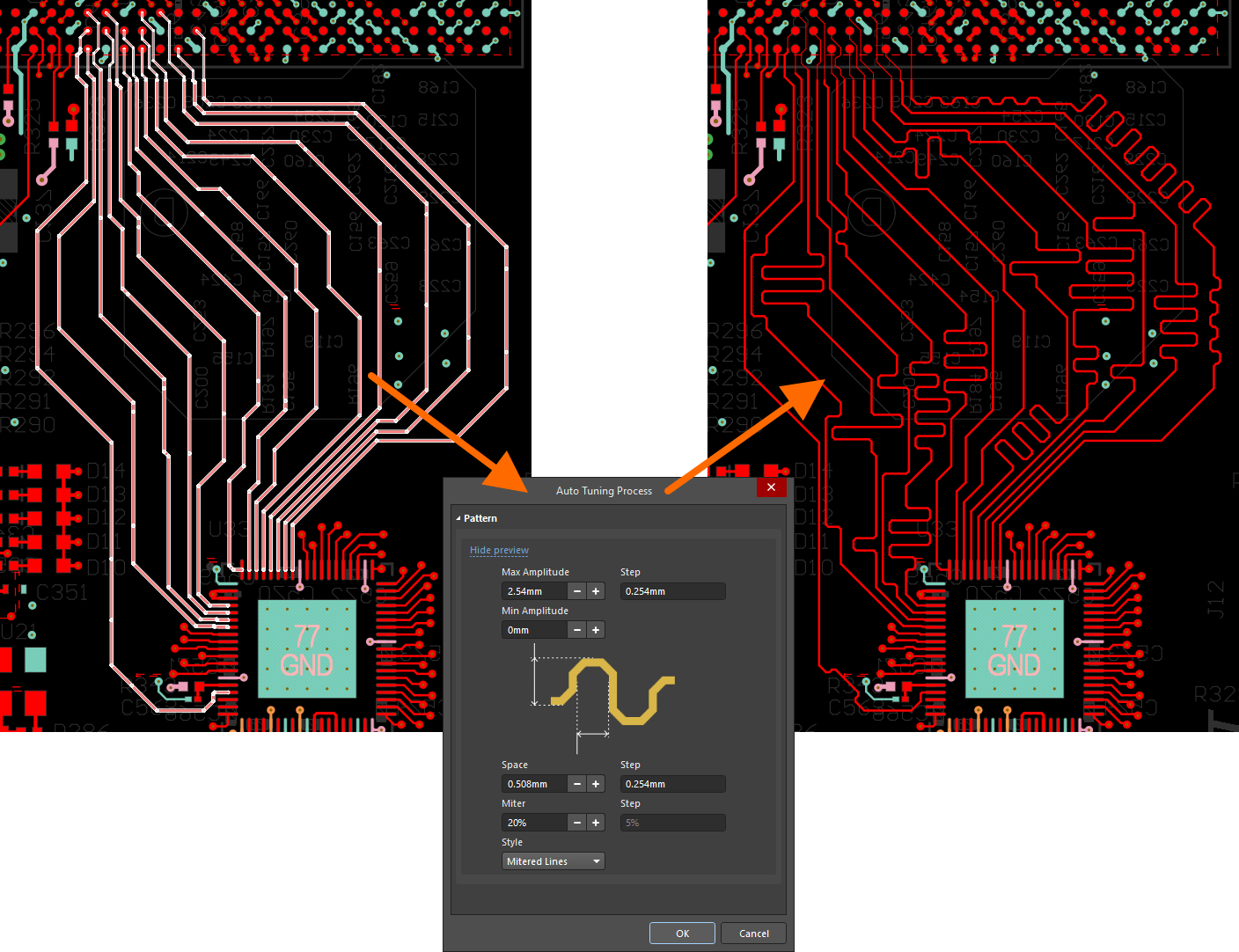
The feature can process:
- Single traces and differential pairs
- Different widths and clearances
- Regular traces and odd angles (except differential pairs)
- Defined high-speed Length and Matched Lengths design rules
- Design rules for nets and for xSignals (pin pairs)
- Routed and signal lengths
This feature is in Open Beta and is available when the
PCB.TraceTuning.AutoTuning option is enabled in the
Advanced Settings dialog.
Update to Length Clipping Behavior during Interactive Tuning
When interactively tuning a net or differential pair in From Rules mode with the Clip to Target option enabled in the Properties panel, the tuning pattern length is automatically clipped once the length slightly below the target (but within the defined tolerance) is achieved. That allows for preventing potential violations of Matched Length design rules.
Updates to PCB CoDesign
Updated Panel Name
In accordance with the official naming of this feature area, the Compare and Merge panel has been renamed the PCB CoDesign panel.
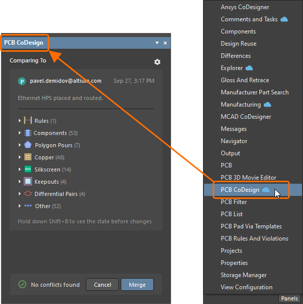
The PCB CoDesign panel and the PCB CoDesign entry in the Panels menu
Added Settings Pop-up
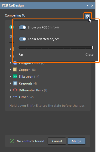
The PCB CoDesign panel now includes a display settings control ( ), giving access to a pop-up to configure whether changes are highlighted on the PCB (the Show on PCB toggle, shortcut: Shift+A) and whether a selected object is zoomed and by how much (the Zoom selected object toggle and slider).
Added Ability to Toggle Between the Current State and Before Changes States
You now have the ability to quickly toggle between the current state and the state before any changes by holding the Shift+B keyboard shortcut. The hint in the panel shows which state is currently active.
❯ ❮
Javascript ID: PCBCoDesign_BeforeAfter
|
Added Support for Pin-to-Pin Connections
To make it easier to understand changes in large nets, copper objects in nets are now split into smaller entities – pin-to-pin connections.
❯ ❮
Javascript ID: PCBCoDesign_PinToPin
|
Enhanced Support for Net Conflict Resolving
To provide better control over net conflicts, you can now choose if local or remote changes should be applied for each object in a net (tracks and vias).
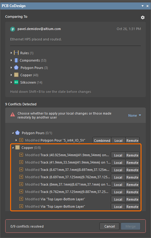
You must be connected to a Workspace to use this feature. Also, note that this functionality is not supported with the Altium Designer Standard Subscription.
Constraint Manager
In this release, a new approach to defining design constraints has been implemented in the form of the Constraint Manager. The Constraint Manager gives both electrical and layout engineers access to the same document-based, spreadsheet-like user interface for the management of net constraints across the design. Accessed from the schematic and PCB editors, the Constraint Manager allows defining electrical clearances between net classes in the form of a class-to-class matrix, as well as physical and electrical rules for nets, differential pairs, and xNets (user-defined signal paths on the schematic side) and their classes. The Constraint Sets expedite the process of defining the constraints for objects that should have the same set of constraints. Also, the Constraint Manager is now command central for managing definitions of differential pairs, as well as net and diff pair classes; there is no need to use design directives on the schematic side for this.
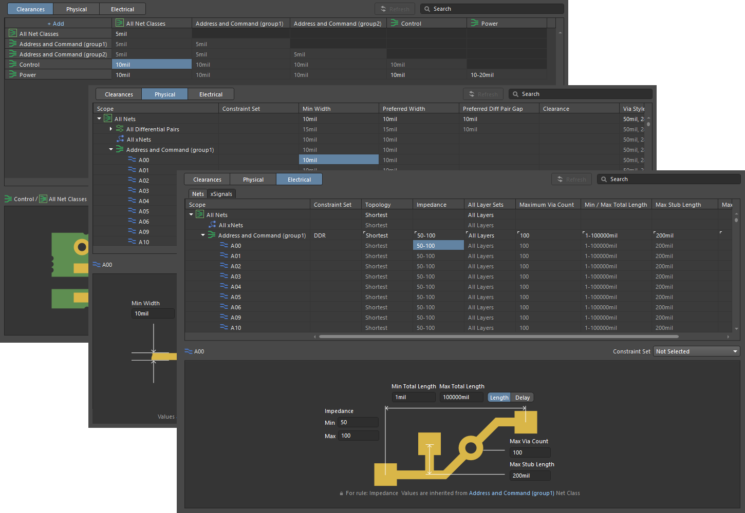
Note that the Constraint Manager is not supported with the Altium Designer Standard Subscription.
This feature is in Open Beta and is available when the
System.ConstraintManager option is enabled in the
Advanced Settings dialog.
Harness Design Improvements
Crimp Assignments
Crimp assignments can now only be modified in the Wiring Diagram, with the corresponding crimp information grayed out/non-editable in the Layout Drawing. Note that this is a temporary solution due to the unidirectional nature of importing changes from the Wiring Diagram to the Layout Drawing (i.e., crimps defined on the Wiring Diagram will always prevail when changes are imported). This will be reversed once full bidirectional synchronization (between the Wiring Diagram and Layout Drawing) for crimps is implemented.
Connection Point Enhancement
When adding objects to a connection point in the Layout Drawing, the option Show only unassigned objects is now enabled by default in the Add Assigned Objects dialog.
License Management UI Enhancements
The License Management view includes the following enhancements in this release:
Data Management Improvement
SiliconExpert Parameter Usage when Creating a Component
When creating a new Workspace library component based on a manufacturer part, the available parameters provided by the SiliconExpert integration can now be selected to be included in the new component.
The SiliconExpert parameters are now listed in the Use Component Data dialog (accessed, for example, by selecting the Save to My Workspace command from the right-click menu of the manufacturer part in the Manufacturer Part Search panel or the Tools » Create from Part Search command from the main menus of the Component editor in its Single Component Editing mode), in which you can apply the parameters to the component as required. Note that the SE Grade and risk parameters (Overall Risk, Lifecycle Risk, etc.) are not included in the Use Component Data dialog.
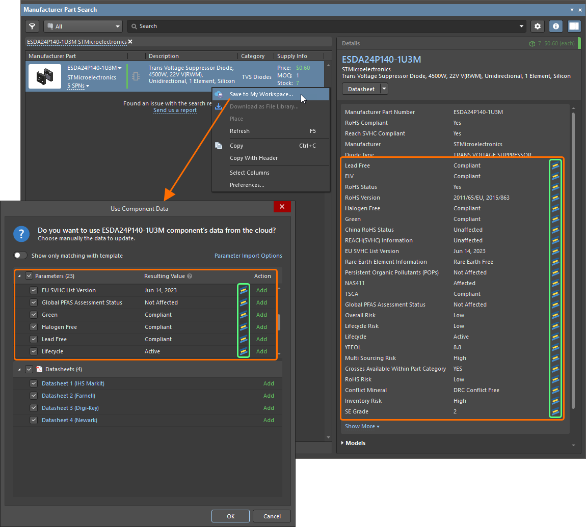
Include SiliconExpert parameters in your Workspace library components.
Mixed Signal Simulation Improvements
-
Components in imported designs or those placed from installed Database libraries are now included in the generated simulation netlist if they have an assigned simulation model.
-
Mixed simulation can now be configured to use a dedicated thread to improve interface response time during simulation. This is available when the Simulation.Threads option is enabled in the Advanced Settings dialog (ON by default).
Altium Designer 23.10
Released: 17 October 2023 – Version 23.10.1 (build 27)
Release Notes for Altium Designer Version 23.10
Key HighlightsExpandCollapse
Schematic Capture Improvement
Improved PDF Generation from Schematics with Objects Over Images
PDF generation from a source schematic document has been enhanced to now provide a clear presentation of text and other drawing objects when placed over a graphic image.
This feature is in Open Beta and available when the
Schematic.ExportPDF.UseBitmapTransparency option is enabled in the
Advanced Settings dialog.
PCB Design Improvements
PCB CoDesign
This release brings a revitalized approach to collaborative design, allowing multiple designers to work concurrently on a PCB in a far more streamlined fashion while greatly minimizing discrepancies and potential reworks. The PCB editor’s new PCB CoDesign feature offers a Git-like approach, with version control provided courtesy of your connected Workspace.
All users access the same Workspace project and commit their changes to a single master branch. Using Altium Designer’s Commenting and Tasks features, you can decide, with your fellow designers, which areas of the board (or layers, nets, or components) you will each work on. As one designer makes a commit, all other collaborators will receive a notification, with the ability to update their local copy with those committed changes before saving their own changes back to the Workspace.
A new-look Compare and Merge panel keeps you apprised of changes to the design, reflecting differences between your local incarnation and that of the last commit. Color coding lets you quickly see which objects have been added, modified and removed. You can also show changes directly within the PCB design space, giving you even greater visual feedback of the comparison. If any conflicts have been detected between objects on the board, such as components, nets and polygons (touched by yourself and another designer), you can choose whether to keep your local changes or accept the remote changes of the latest commit (or for polygon pours, combine objects), then merge to confidently resolve the design overlap.
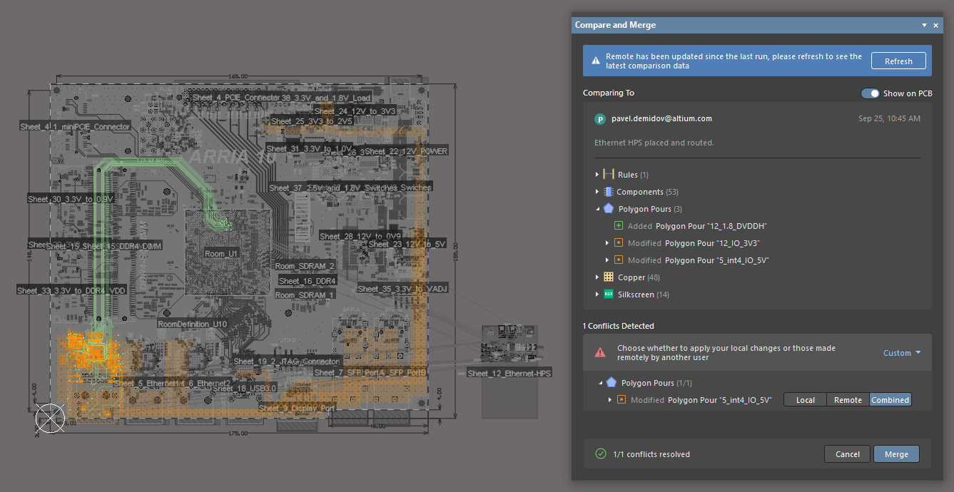
You must be connected to a Workspace to use this feature. Also, note that this functionality is not supported with the Altium Designer Standard Subscription.
This feature is in Open Beta and available when the
PCB.CollaborativeEditing option is enabled in the
Advanced Settings dialog.
Any Angle Retrace
You can now retrace any angle single-ended traces. When you set the Hugging Style option to Rounded in the Gloss And Retrace panel, you can access the Retrace Parameters region to select rule-based width mode for traces to be retraced and enable preserving the route path. Note that this mode does not increase trace width if that would create a clearance violation.
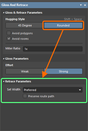
Set Hugging Style to Rounded in the Gloss And Retrace panel to configure retracing of any angle single-ended traces.
This feature is in Open Beta and available when the
PCB.Routing.AnyAngleRetrace option is enabled in the
Advanced Settings dialog.
Harness Design Improvements
Added Annotation for Harness Objects
You can now use the annotation feature to apply desired designators to supported objects on both the Wiring Diagram and Layout Drawing. Supported objects are:
- Wiring Diagram: Wire, Splice (Tap), No Connect, Cable
- Layout Drawing: Connection Point, Layout Label, Harness Bundle
The following commands from the Tools » Annotation menu can be used to annotate the Wiring Diagram and Layout Drawing:
- Annotate Schematics
- Reset Schematic Designators
- Reset Duplicate Schematic Designators
- Annotate Schematics Quietly
- Force Annotate All Schematics
An example of annotating the Wiring Diagram (using the Annotate Schematics command) and the Layout Drawing (using the Annotate Schematics Quietly command) is shown in the video below.
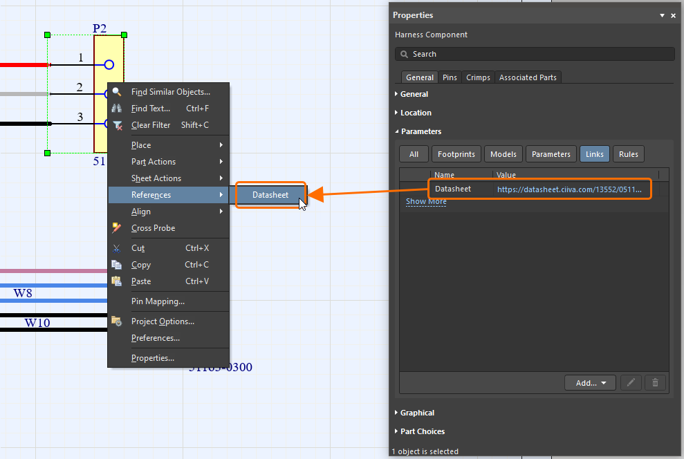
A References sub-menu has been added to the right-click menu for harness components in the Wiring Diagram and the Layout Drawing. The option appears on the right-click menu if a link has been added to the harness component in the Parameters region of the Properties panel. Click an entry in the sub-menu to open its target link.
Added Properties Command for Objects
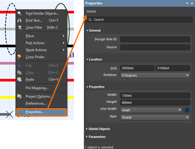
A Properties command has been added to the right-click context menu for objects in the Wiring Diagram and Layout Drawing, allowing for quick access to properties in the Properties panel.
Data Management Improvements
Ability to Inherit a Component Template
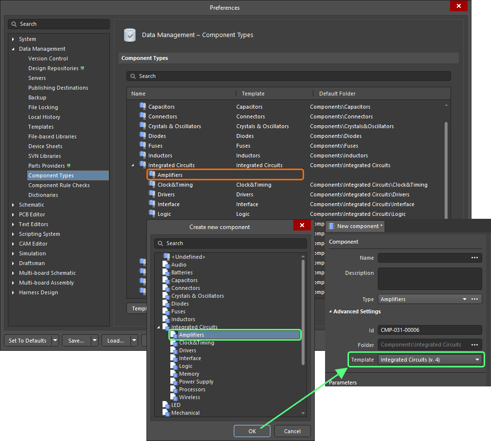
This feature allows you to use a component template from the root component type if the sub-type does not have a component template linked. When building a hierarchy of component types, component sub-types will now inherit the component template assigned to the root/parent component type.
In the example shown below, the Amplifiers component type has no assigned template, so the component template linked to the parent component type (Integrated Circuits) is used when a new component of the Amplifiers component type is created.
This feature is in Open Beta and available when the
UI.ComponentTemplateInheritance option is enabled in the
Advanced Settings dialog.
Redesigned 'Where Used' Region of the Components Panel
The Where Used region of the Components panel has been redesigned. The region now includes 'where used' information in relation to Reuse Blocks stored as part of a connected Workspace's library.
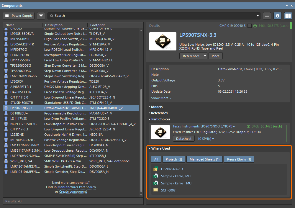
Note that the tabs will only be displayed now if an entity exists in the Workspace that uses the selected component.
Ability to Copy Component History
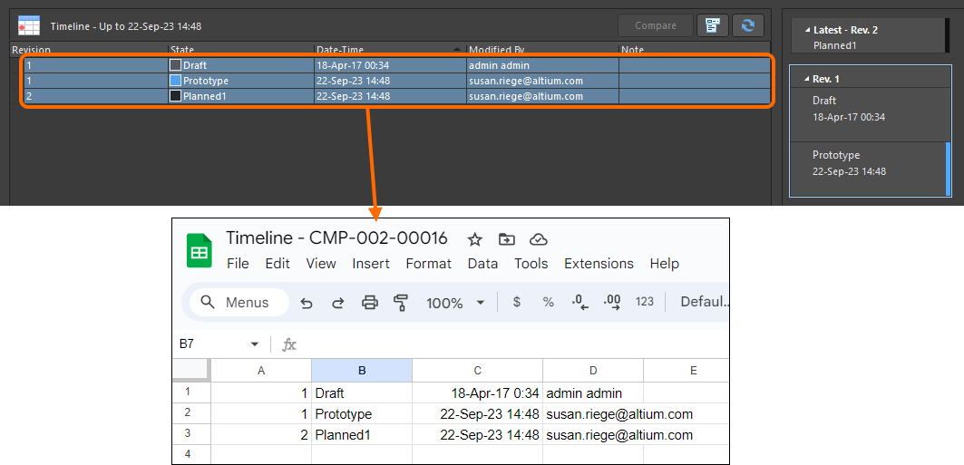
It is now possible to copy component historical data from the Timeline of the Detailed Item View. Use Ctrl+C to copy the selected data from the Timeline and Ctrl+V to paste the data where required (e.g., into a spreadsheet).
Circuit Simulation Improvement
Added TABLE and PWL Functions
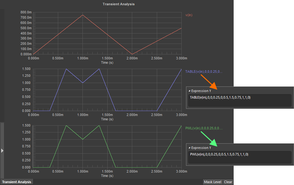
The TABLE and PWL functions can now be used in expressions for output waveforms when configured in the Add Output Expression or Edit Waveforms dialog. Both functions are available in the Miscellaneous category of these dialogs.
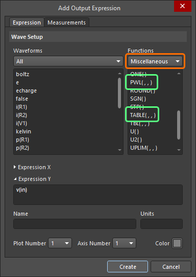
The TABLE(x,a,b,c,d,...) and PWL(x,a,b,c,d,...) interpolate a value for x based on a look-up table given as a set of pairs of points.
Features Made Fully Public in Altium Designer 23.10
The following features have been taken out of Open Beta and have transitioned to Public in this release:
Altium Designer 23.9
Released: 14 September 2023 – Version 23.9.2 (build 47)
Release Notes for Altium Designer Version 23.9
Key HighlightsExpandCollapse
Harness Design Improvements
Enhanced Physical View Zoom Functionality
Zoom functionality has been enhanced when defining a physical view on the Layout Drawing. For both Solid and Wireframe styles, the Zoom value now defines the size of the model view's green bounding box in the design space, and the model view now always fits in the bounding box. Because the size of the bounding box is no longer independently definable, the Width and Height fields have been removed from the Properties panel.
❯ ❮
Javascript ID: Harness_LD_Component_Zoom_AD23_9
|
Shortcuts for Placing Wires and Bundles
Shortcuts have been added for placing a wire (Shift+W) in the Wiring Diagram and a bundle (Shift+B) in the Layout Drawing.
License Management UI Enhancements
The updated License Management view includes a number of enhancements in this release.
-
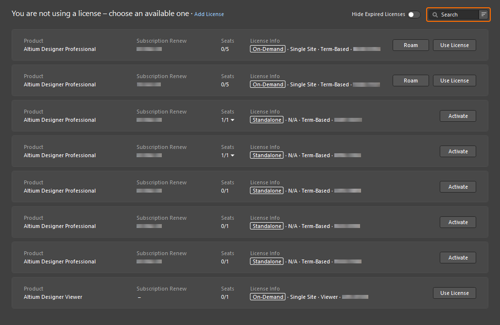
License type "labels" have been added to quickly (and visually) distinguish between licenses in the listing.

-
The Search field and the sorting control now display when there are more than seven licenses in the listing.
Data Management Improvements
Ability to Open a Manufacturer Part in Octopart
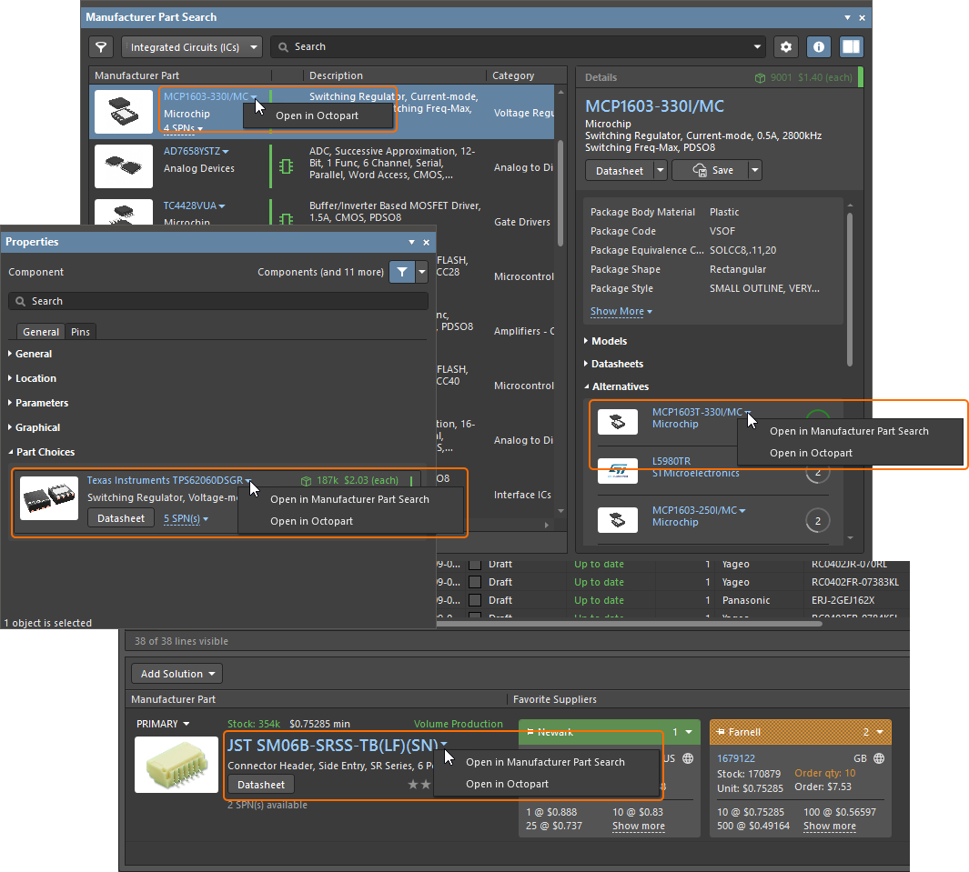
The menu associated with a manufacturer part (a part choice, an alternative in the Manufacturer Part Search panel, or a solution in an ActiveBOM document) now includes not only an option to open this part in the Manufacturer Part Search panel but also an option to open a page for this part in the Octopart site in your browser. Click the drop-down menu icon at the right of the part name to access the command.
Ability to Migrate from SVN to Git
When Altium Designer is connected to an Enterprise Server Workspace and a design project is stored in an SVN repository managed through the Workspace's Version Control Service, you can now migrate this project from the SVN repository to the Workspace's built-in Git repository (Versioned Storage). To do this, open the project from the Workspace in Altium Designer, right-click its entry in the Projects panel, then select the History & Version Control » Migrate Project to Altium Versioned Storage command from the context menu. Alternatively, click the Migrate to Server Versioned Storage button in the Project Options dialog.
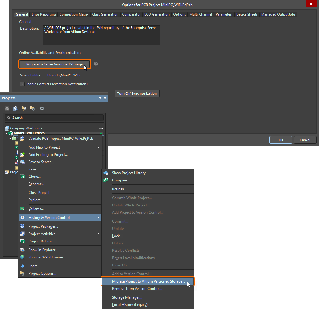
After following the prompts, which include making a final VCS commit, the project will be migrated to the version control of the Workspace Git repository.
Importer/Exporter Improvements
OrCAD and Allegro Import Improvements
This release delivers a number of key improvements and fixes in relation to the import of OrCAD and Allegro design files into Altium Designer. These include:
- Support for customized port connectors defined in OrCAD design schematics.
- Parameters defined in the title block of an OrCAD schematic are now treated/behave as true document parameters.
- Components on OrCAD schematics now faithfully keep their fill coloring and comment placement on the generated Altium Designer schematics.
- When importing an Allegro
.dra file, SMD pads are now imported correctly as Simple (rather than Full Stack), with correct sizing presented in the Properties panel.
- Import of an Allegro
.brd file that has been created in v17.4 and then saved in 17.2 format (the same version as that of the Extracta installation) will now complete successfully.
Altium Designer 23.8
Released: 15 August 2023 – Version 23.8.1 (build 32)
Release Notes for Altium Designer Version 23.8
Key HighlightsExpandCollapse
Schematic Capture Improvement
Ability to Change Rectangle Border Line Style
You can now change the line style of the border of rectangles in a schematic or schematic symbol document. Use the Line Style drop-down in the Properties panel to select the desired style.
❯ ❮
Javascript ID: SCH_Rectangle_LineStyles_AD23_8
|
PCB Design Improvements
Custom Paste/Solder Masks
This feature allows you to create custom shapes on paste and solder mask layers of pads in PCB designs and PCB footprints.
As part of this improvement, the pad stack configuration UI in the Properties panel has been updated. From the updated grid in the Pad Stack region of the panel, you can configure the stack of the selected pads on different layers as required, including the shapes on the paste mask and solder mask layers.
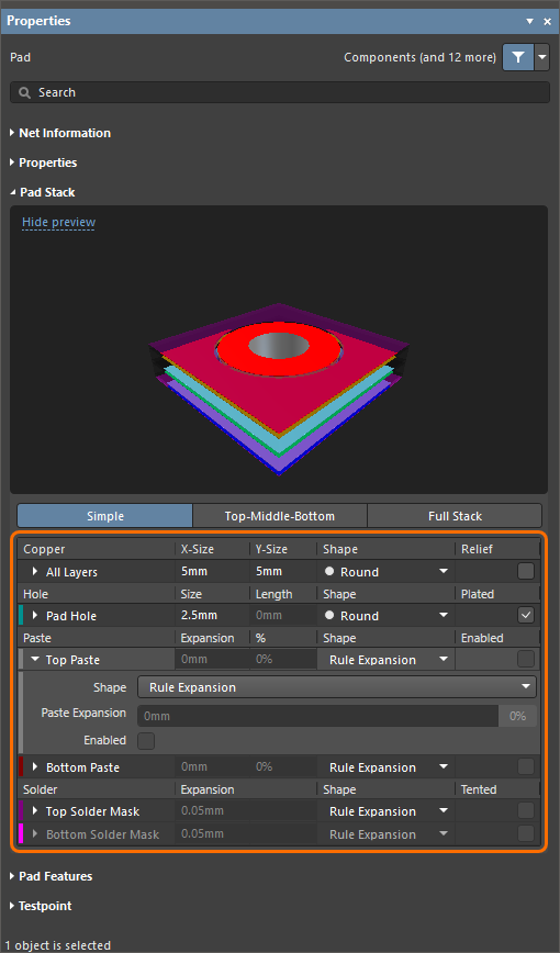
The updated UI of the Pad Stack region of the Properties panel (when one or more pads are selected) with the Top Paste layer region expanded as an example.
A custom shape on the paste or solder mask layer can be defined by selecting Custom Shape from the Shape drop-down, then clicking the Edit button in the Properties panel, and then defining the shape of the region on this layer by either editing the existing or placing new primitives (tracks, arcs, fills, etc.). Copying and pasting primitives while defining the shape is also supported.
|
|
An example of defining a custom shape on the Top Solder Mask layer in the Properties panel. When the pad is selected, choose the Custom Shape option from the Shape drop-down for the required layer.
When the layer region is expanded, click the Edit button to enter the editing mode of the shape on that layer.
When the shape is defined as required, click the Complete button at the top of the Properties panel (or use the Shift+C shortcut when in the design space).
The result of defining the custom shape on the Top Solder Mask layer.
|
Alternatively, create the desired custom shape on the paste/solder mask layer using a combination of track, arc, fill, and solid region primitives, then add those selected primitives to the pad (on that paste/solder mask layer) using the new Add Selected Custom Masks to Pad command (from the right-click Pad Actions sub-menu).
|
|
An example of defining a custom shape on the Top Paste Mask layer using placed primitives. A pad with the disabled top paste mask shape is shown.
Place primitives on the solder and/or paste mask layers defining pad shapes on these layers as required. Four fills placed on the top paste mask layer are shown.
When the placed primitives are selected, right-click on the selection then choose the Pad Actions » Add Selected Custom Masks to Pad command from the right-click menu.
Click the pad to which the primitives should be added.
The primitives will be added to the current solder/paste shapes of the selected pad. The Custom Shape entry will be shown for the affected layers.
|
Other options for defining the paste/solder mask shape are also available in the Shape drop-down.
- Rule Expansion - the paste/solder mask expansion will be defined by an applicable Paste Mask Expansion / Solder Mask Expansion design rule.
- Manual Expansion - the expansion value will be defined as an attribute of the selected object or one of the predefined shapes.
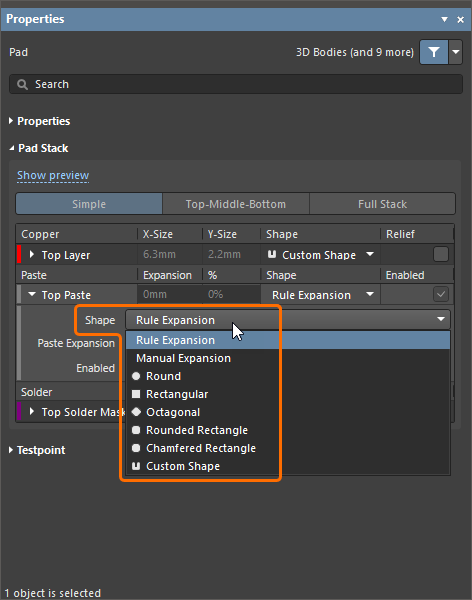
The paste/solder mask shapes other than Custom are also available in the Shape drop-down.
Custom paste/solder mask shapes are supported in Draftsman documents and Gerber, Gerber X2, ODB++, and IPC-2581 outputs.
To support 'pin-in-paste' and 'thru-hole reflow' technologies, the ability to enable the paste mask for thru-hole pads has also been added. To enable paste mask on the top and/or bottom board sides for thru-hole pads, use the Use Top Paste and Use Bottom Paste options in the Paste Mask Expansion design rule or define the required expansion value for selected pads manually when the Manual Expansion option is chosen as the pad Shape in the Properties panel.
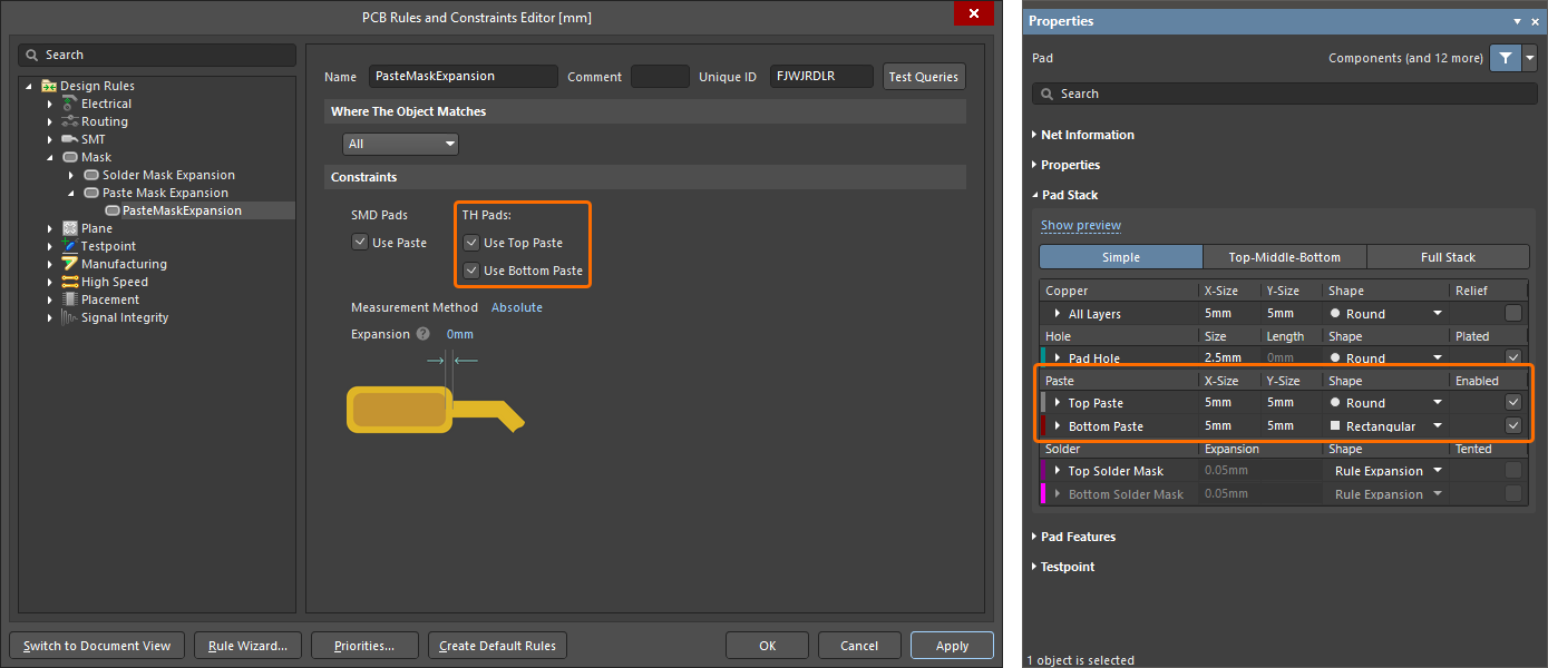
Define the required expansion value of the paste mask using the Paste Mask Expansion design rule or the Paste options in the Properties panel (with one or more pads selected).
An example of a board region that includes some thru-hole pads for which the paste mask is enabled and the Paste Mask layer for the same region (in 2D and 3D) is shown below.
The paste mask layer for thru-hole pads is supported in Draftsman documents and Gerber, Gerber X2, ODB++, IPC-2581, and PCB Print outputs.
This feature is in Open Beta and is available when the
PCB.Pad.CustomMasks option is enabled in the
Advanced Settings dialog.
Added New Special Strings
The following pre-defined, system-based special strings have been added and are available for use on a PCB document.
.BlindVia_Count |
.Board_Height |
.Board_Width |
.BuriedVia_Count |
.ComponentMixed_Count |
.ComponentSMD_Count |
.ComponentThru_Count |
.CopperInner_Weight_Max |
.CopperOuter_Weight_Max |
.Hole_Size_Min |
.Hole_Size_Num |
.Layer_Count |
.MicroVia_Count |
.PadSMD_Count |
.PadThru_Count |
.SolderMask_Bottom |
.SolderMask_Top |
.StackedVia_Count |
.Thru_Via_Count |
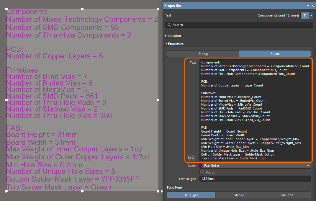
The above new special strings are also available for a Draftsman document.
Note that:
- Draftsman special strings are prefixed with "
=" rather than "."
- The new special strings are available in Draftsman once the data has been imported from the PCB (Tools » Import Changes From <PCBDocumentName>.PcbDoc).
- The Board Height and Board Width special strings have a slightly different format in Draftsman, namely;
=BoardHeight & =BoardWidth.

For more information, refer to Working with Draftsman Drawing Annotation Features.
Added Ability to Keep Room Orientation
The ability to control whether or not the rotation of the chosen source room is copied to the desired destination room when using the Copy Room Formats feature has been added. Altium Designer detects the orientation of rooms (by the rotation angle of the component with the largest pin number or the largest area within the room) and uses that to rotate the destination room. The process is as follows:
- Use the Design » Rooms » Copy Room Formats command from the main menus.
- Use the mouse to move the crosshairs to the desired source room, then click to select it.
- Move the crosshairs to the destination room, then click to select it.
- Disable the Copy Room Orientation option in the Confirm Channel Format Copy dialog that opens to keep the original orientation of the destination room(s).
- Configure other options in the dialog as required, then click OK. The format of the source room will be copied to the destination room(s).
- Continue selecting destination rooms or right-click to finish.
Draftsman Improvement
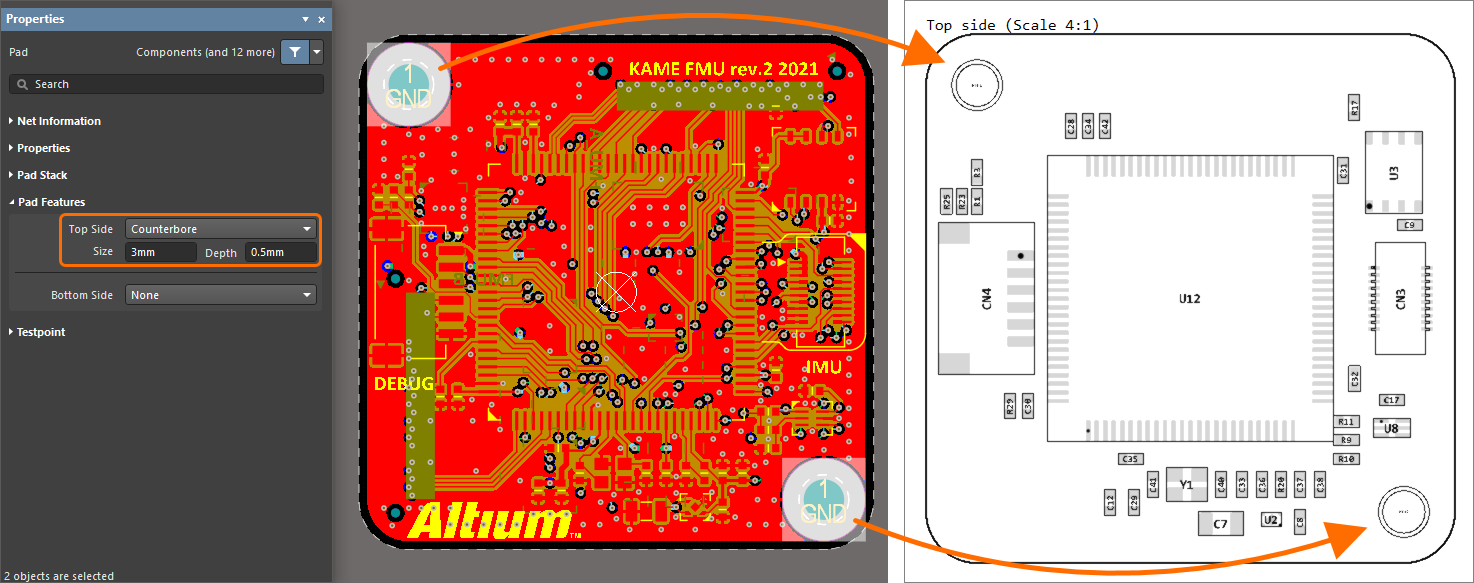
Added Counterhole Support to Board Assembly View
In this release, support for counterholes has been implemented for Draftsman's Board Assembly View. If the source PCB has thru-hole pads with counterhole features applied, these pads will be properly shown in the Board Assembly View for the PCB in the Draftsman document.
Harness Design Improvement
Introduced Harness ERC
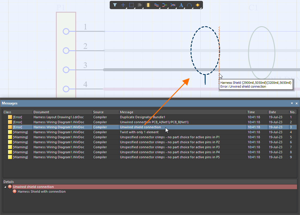
Electrical Rules Checking (ERC), with a variety of supported violation types, is now available for the Wiring Diagram and Layout Drawing of a Harness Design project. Similar to validation for a PCB design project, reporting levels are configured as part of the options for the Harness Design project (Project » Project Options).
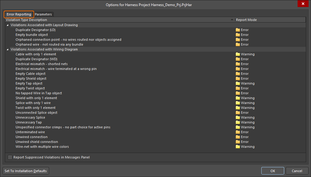
After performing project validation (Project » Validate Harness Project), results are presented in the Messages panel, as well as graphically within the design space.
Updated License Management UI
In this release, the user interface of the License Management view has been redesigned with streamlined and intuitive controls applicable to Altium Designer users and administrators of an Altium account. The main features of the new user interface are:
- Streamlined representation of information about the connected Altium account and available licenses.
- Warning messages for licenses and their subscriptions that are expired or that will expire soon.
- Ability to contact Altium account administrators to notify them of licensing issues, for example, an expired license, an expired subscription, or a lack of license seats.
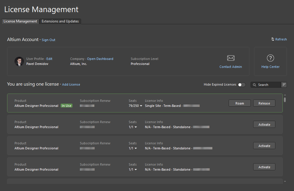
The redesigned user interface of the License Management view
Also, warning messages will be displayed when connecting to a Workspace if your current Altium Designer Subscription level is higher or lower than that of the organization to whose Workspace you are connecting.
This feature is in Open Beta and is available when the
System.LicenseManagement2023 option is enabled in the
Advanced Settings dialog.
Data Management Improvement
Draftsman Documentation Output Job Enhancement
OutJob labels have been modified when adding Draftsman documentation outputs to an OutJob file (*.OutJob). A single entry titled 'Draftsman' is available with the data source that is applicable to the parent project type listed in the sub-menu.
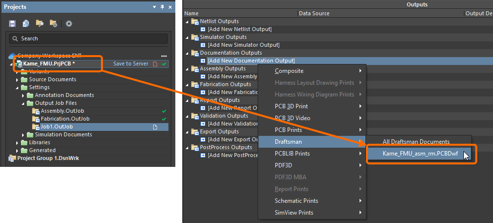 Displaying a PCB project Draftsman documentation output data source. Hover over the image to see a Harness project Draftsman documentation output data source.
Importer/Exporter Improvements
OrCAD Import Improvements
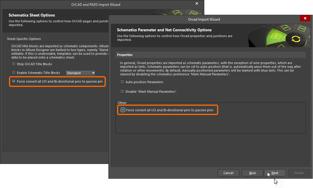
Added Ability to Force Pin Conversion
During the import of OrCAD designs, you can now force all I/O and bi-directional pins to be converted to passive pins. During the import process using the Import Wizard (File » Import Wizard), the Force convert all I/O and Bi-directional pins to passive pins option has been added to the Schematics Parameter and New Connectivity Options page (when Orcad Designs and Libraries Files is selected as the file type to import) and on the Schematics Sheet Options page (when Orcad and PADS Designs and Libraries Files is selected as the file type to import).
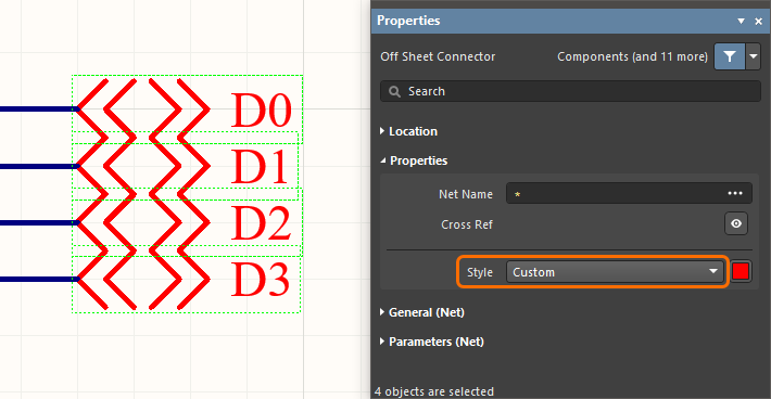
Added Custom Off Sheet Connector Support
When an OrCAD design is imported through the use of the Import Wizard, customized bi-directional off-sheet connectors are now supported on the generated schematic document.
Simulation Improvement
Support for Transient Modeling
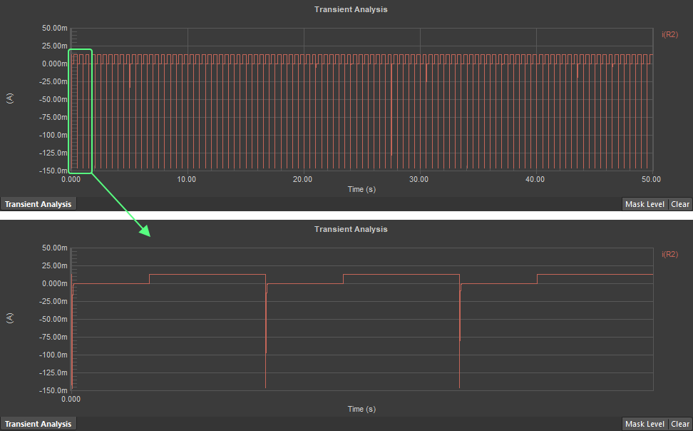
The simulator has been enhanced in this release to support models of ISO 7637-2 and the simulation of repeated bursts of transients through the extension of the EXP function in independent sources. The extended syntax for the EXP function:
EXP(V1 V2 Td1 Tau1 Td2 Tau2 Tpulse Npulse Tburst),
where:
Tpulse – pulse periodNpulse – the number of pulses per burstTburst – the repeat burst period
The image below shows an example of an oscillogram of a source using the EXP function with these parameters.
Altium Designer 23.7
Released: 19 July 2023 – Version 23.7.1 (build 13)
Release Notes for Altium Designer Version 23.7
Key HighlightsExpandCollapse
Harness Design Improvement
Added Support for 'No Connect' Objects Within a Cable
Previously, a No Connect object within a Harness Cable had to be added to a Connection Point in the Layout Drawing. No Connect objects in a Harness Cable are now supported without the need to add them to a Connection Point.
|
|
A cable in the Wiring Diagram document contains unconnected wires (W_NC1 and W_NC2).
While the No Connect objects are not assigned to the connection points in the Layout Drawing document...
The bundle correctly recognizes all objects of the cable (including wires W_NC1 and W_NC2).
|
Multi-board Improvements
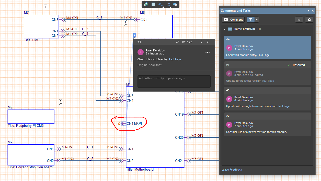
In Multi-board schematic documents, you can now add and manage comments using the same approach as in the other editors that support comments, such as the schematic and PCB editors.
Cross-probe to Linked Harness Project
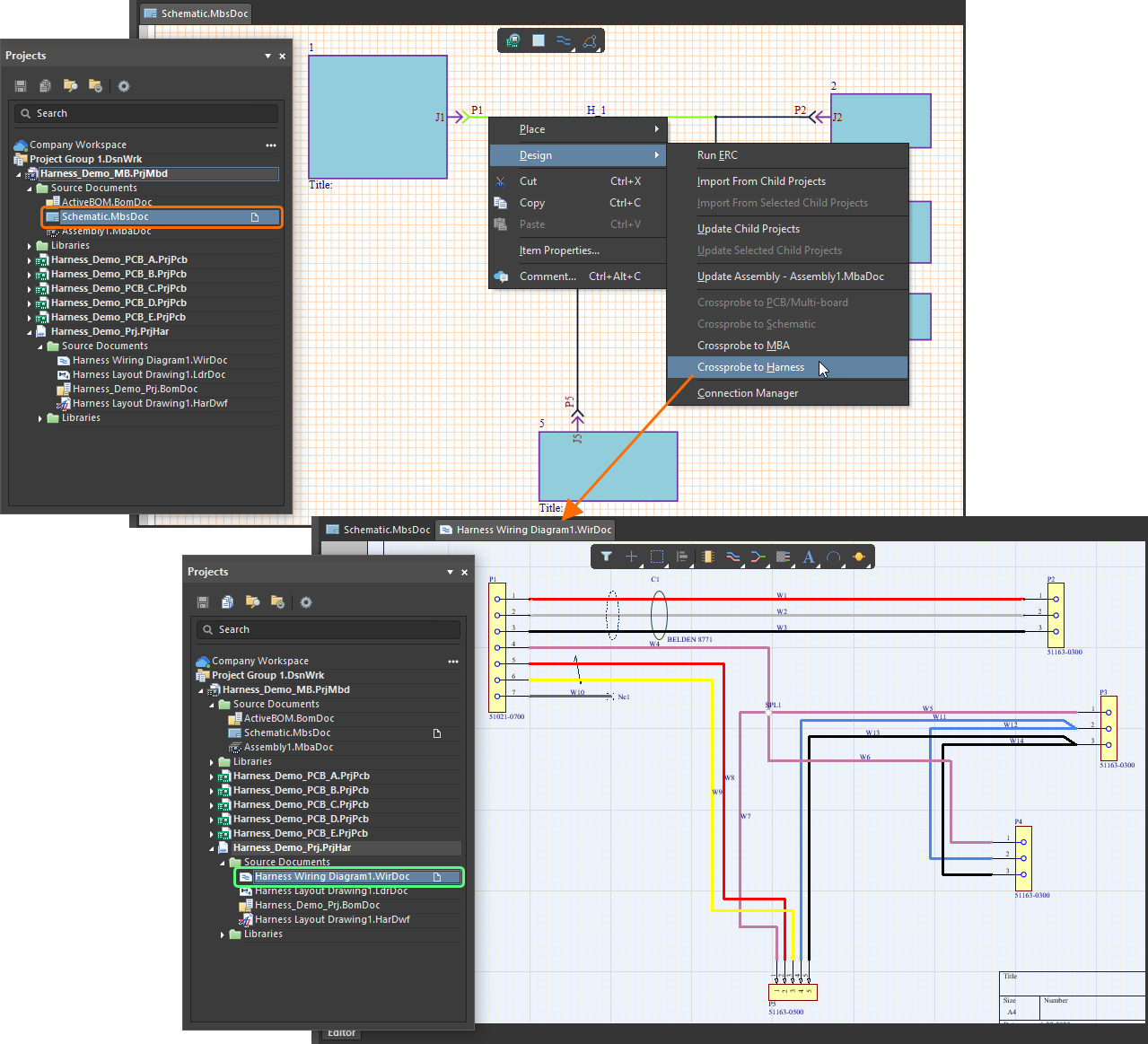
With this release, you can cross-probe from a multi-board schematic document (*.MbsDoc) to a linked harness project (*.PrjHar). Use the Design » Crossprobe to Harness command from the main menus or from the right-click menu of a multi-board schematic when the required harness connection is selected. The wiring diagram document of the associated harness project will open.
Data Management Improvement
Excluding Part Choices from BOM
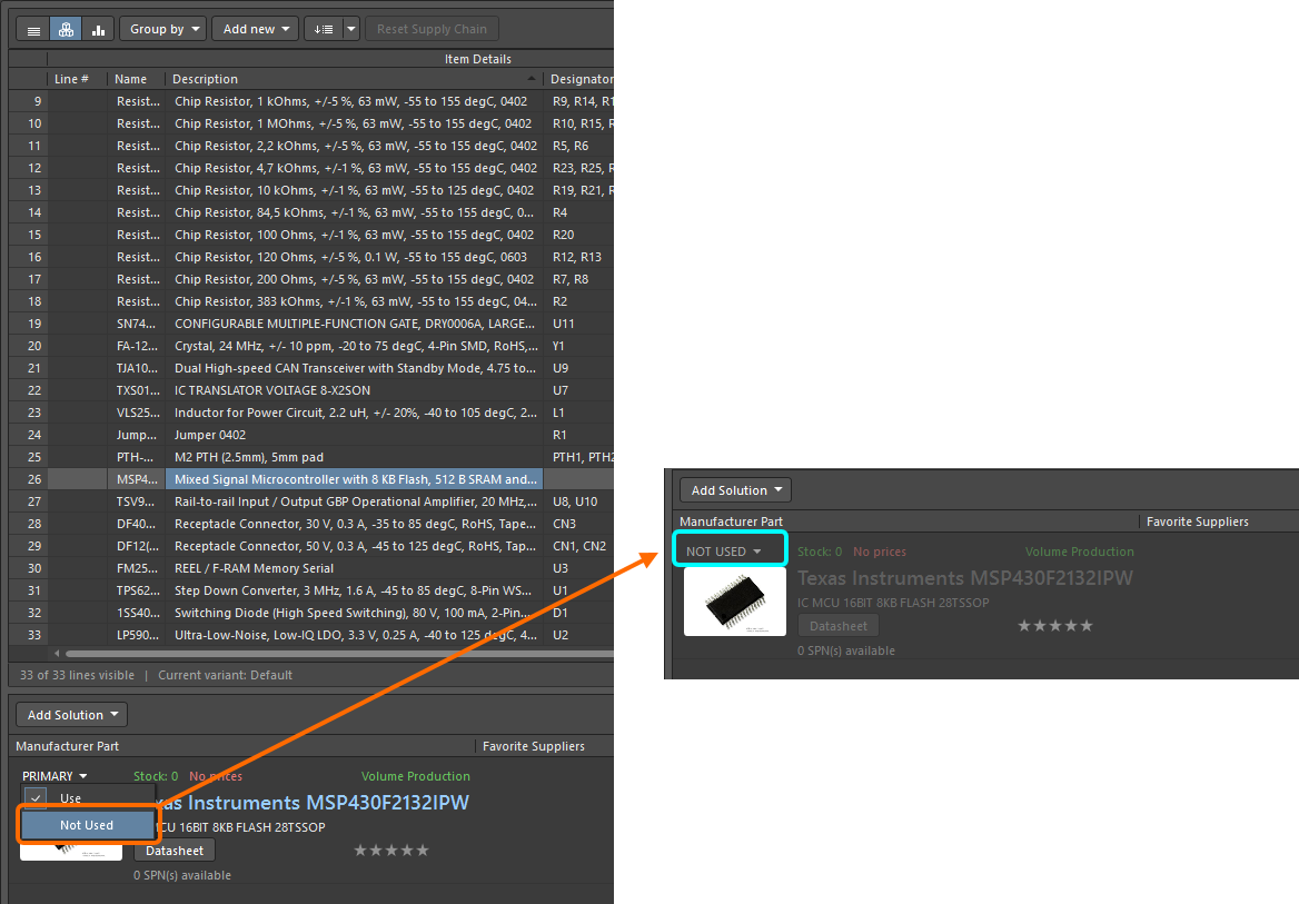
You now have the capability to exclude a Part Choice defined for a component from the project in the ActiveBOM document. This is useful when a component has many different part choices; you can exclude any that you do not want in your project. To exclude specific part choices, in the BOM document (*.BomDoc), select Not Used in the drop-down associated with PRIMARY or SECONDARY. The drop-down will now display NOT USED. Please note that if you exclude the primary part choice, the secondary part choice becomes primary.
An excluded part choice will not appear in the generated BOM, and it will not be used in price calculations or as part of BOM checks.
If your requirements change, you can change Not Used to Use using the drop-down.
Circuit Simulation Improvements
Added Inductance Current Support
Added support for using currents through inductances in a functional source value expression.
Added Support for the Initial Condition Directive in Subcircuits
The initial condition directive (.IC) defined within a subcircuit is now supported and can be processed/applied.
When viewing simulation results, it is now possible to select multiple waveforms in a plot using Shift+Click. This might be useful to compare some waveforms in a waveform-dense plot. Multiple selected waveforms (selected in the same or different plots) can be moved to another plot using drag-n-drop.
Altium Designer 23.6
Released: 15 June 2023 – Version 23.6.0 (build 18)
Release Notes for Altium Designer Version 23.6
Key HighlightsExpandCollapse
PCB Design Improvements
Additional Clipping Options for Silkscreen Preparation
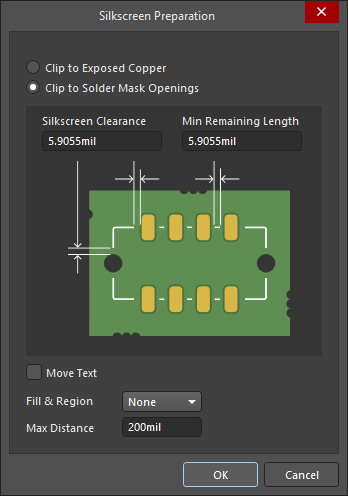
Options have been added to the Silkscreen Preparation dialog (Tools » Silkscreen Preparation) that allow you to clip objects to exposed copper (Clip to Exposed Copper) and clip objects to solder mask openings (Clip to Solder Mask Openings). The new options are only available when the Use Design Rules option is disabled, as shown in the image below. Some options of the dialog have also been rearranged or renamed to optimize usage.
|
|
A region of a board before silkscreen preparation processing
A region of a board after silkscreen preparation processing with the Clip to Exposed Copper option enabled
A region of a board after silkscreen preparation processing with the Clip to Solder Mask Openings option enabled
|
The new options are also available in the dialog when accessed from the PCB footprint editor. The new options are always accessible when accessed this way since design rules do not pertain to the PCB footprint editor.
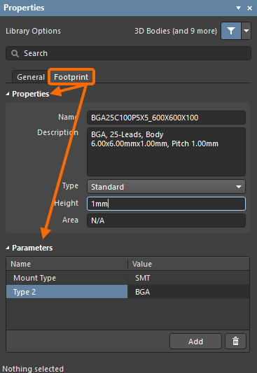
User-defined parameters for footprints are now supported in Altium Designer. Previously, a footprint could have a set of parameters; however, only the Description field was available without any capability to add more information.
To streamline the process of configuring footprint properties, a Footprint tab has been added to the Library Options mode of the Properties panel. The Library Options mode is accessed from a PCB library document (*.PcbLib) when no objects are selected in the design space. The Footprint tab displays the Properties and Parameters of the active footprint.
You can also see defined footprint parameters at the PCB component level in the Properties panel in the Component mode on the Parameters tab as shown below.
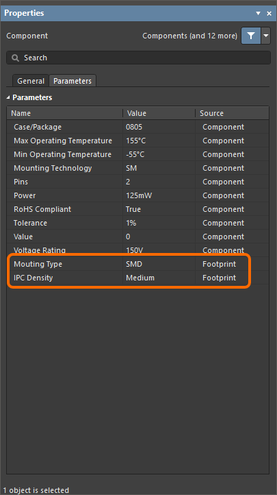
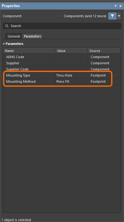
The parameters defined at the footprint level can be seen in the Properties panel in its Component mode when the component is placed on a PCB.
In support of footprint parameters, various keywords have been added to the Query Language (FootprintParameterValue, HasFootprintParameter and HasFootprintParameterValue). These keywords can be used to filter the required components in the design space or scope design rules.
Footprint parameters are supported by Altium Designer’s Comparison engine. When updating footprints from file-based and database libraries, the Update From PCB Libraries dialog will include a new Parameters tab listing parameter differences. When applying changes directly from the PCB footprint editor, the Component(s) Update Options dialog will include a new Footprint Parameters option.
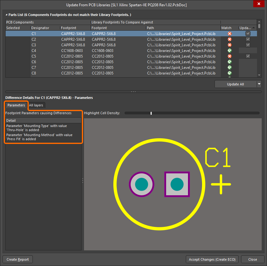
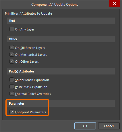
Footprint parameters of components placed on a PCB will be propagated to footprints in libraries generated by the Make PCB Library or Make Integrated Library command of the PCB editor's main menu.
Footprint parameters are also supported for generated Pick and Place and ODB++ output.
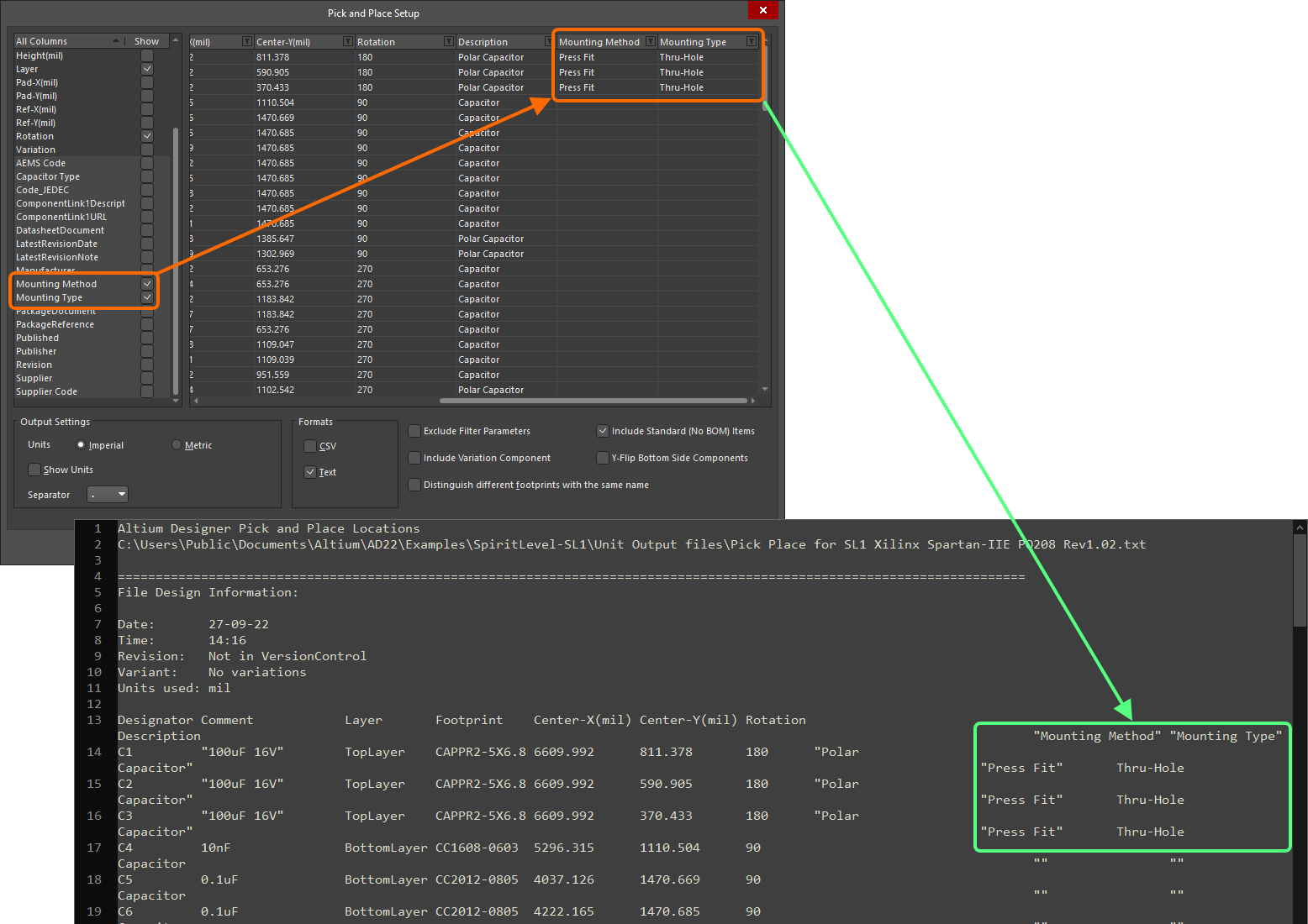
An example of generated Pick and Place output that includes footprint parameters selected in the Pick and Place Setup dialog
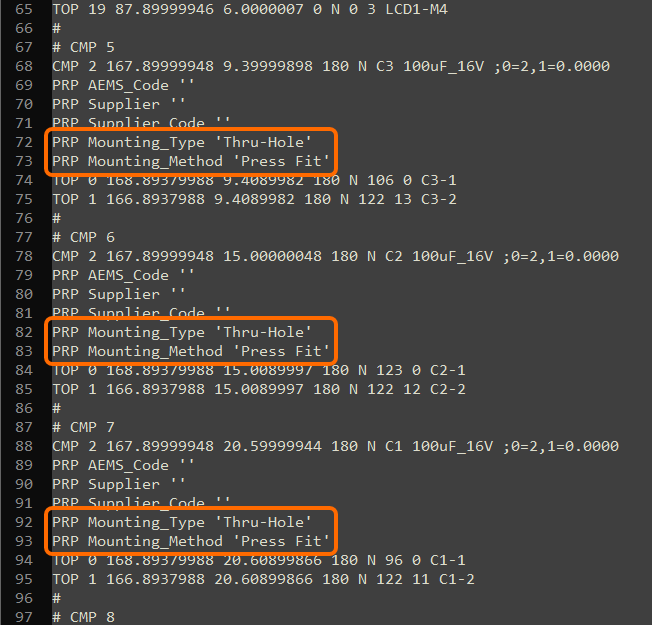
An example of generated ODB++ output (the components file) that includes footprint parameters
Altium MCAD CoDesigner supports the placement of native MCAD components in the MCAD according to the configured linking. In some cases, several footprints with different models are linked to one component (e.g., a LED that can be mounted on a PCB in two ways: vertically, with straight legs, or horizontally, with bent legs). Using the footprint parameters, you can now refer to the different MCAD models from those different footprints. Learn more about
Linking Native ECAD and MCAD Design Components.
This feature is in Open Beta and is available when the
PCB.FootprintParameters option is enabled in the
Advanced Settings dialog.
Harness Design Improvements
Added Support for Templates
The ability to save harness documents as templates has been added. Saving the Wiring Diagram, Layout Drawing and Draftsman Layout as templates is useful when creating new Harness Design projects by removing the need to reconfigure them each time. To save harness documents as templates, right-click on the document in the Projects panel, then select Save As. In the File Explorer window that opens, select the template type (*.<xxx>Dot) in the Save as type drop-down.
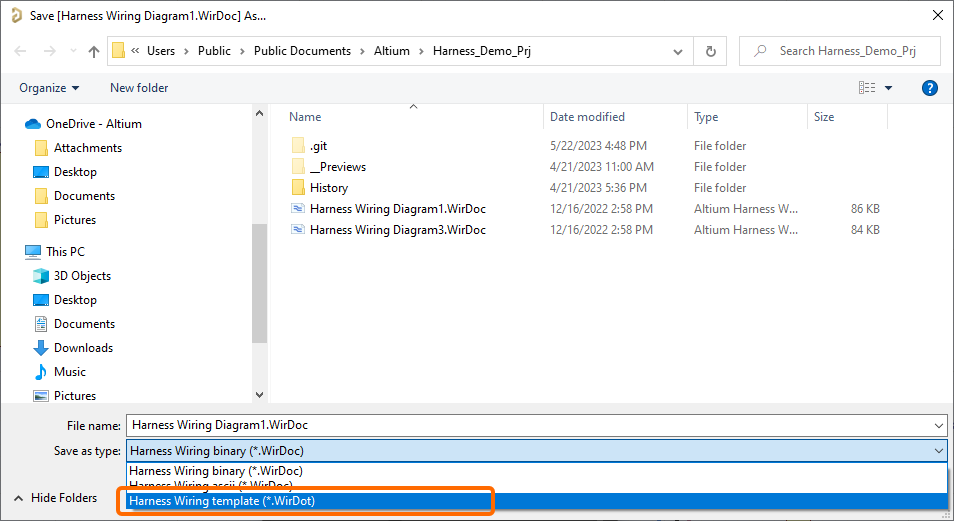
A Harness project can also now be copied to the Templates folder for use as a local template. For a default installation, the Templates folder path is \Users\Public\Documents\Altium\AD<Version>\Templates. When a new Harness Design project is created, you can use your locally-saved template for the new project. In the Document Options mode of the Properties panel (accessed when no objects are selected in the design space), select Template in the Formatting and Size region, then select the desired template from the Template drop-down.
Added 'Isometric' View for Physical Models
Starting with this release, physical models can be displayed as an 'isometric view,' which can help to more clearly represent the 3D object in your Layout Drawing. In the Physical View drop-down of the Harness Component mode of the Properties panel (accessed when a harness component is selected in the design space), select the desired view in the Side drop-down. Scroll through the below images to view some of the settings with the corresponding results in the design space.
Enhanced Harness Covering Properties
For a Harness Covering object, you can now define its size relative to the size (Line Style) of the bundle it is covering using the Size drop-down in the Harness Covering mode of the Properties panel. Scroll through the images below to see examples of different sized Harness Coverings with various Harness Bundle Line Styles.
Another enhancement for harness coverings is that they can now be patterned. In the Fill Style region of the Properties panel, select Pattern, then use the Pattern drop-down to choose the desired weave color (black, yellow or red).
Connections Between Multi-Board Projects Using Harness Connectors
It is now possible to use harness connectors to make connections between multiple multi-board projects that are in a nested configuration.
|
|
A child Multi-board project has a harness connector whose entry has the System Entry option enabled.
When changes are imported to the parent Multi-board project, this harness connector will be added as a module entry of the child project's module.
|
Circuit Simulation Improvement
Added FSTIM PSpice Digital Model Primitive
Support for the file stimulus (FSTIM) PSpice digital model primitive has been added.
Features Made Fully Public in Altium Designer 23.6
The following features have been taken out of Open Beta and have transitioned to Public in this release:
Altium Designer 23.5
Released: 18 May 2023 – Version 23.5.1 (build 21)
Release Notes for Altium Designer Version 23.5
Key HighlightsExpandCollapse
PCB Design Improvements
Added New PCB Section View
To provide better insight into the layout and structure of a complex PCB, the Section View functionality has been implemented for the PCB editor. Using the Section View is helpful when it is required to reveal details within a PCB that might typically not be visible, for example, when smaller SMD components are placed under larger components or mechanical parts, which could make operations such as component movement and distance measuring difficult.
The Section View functionality is available in the PCB editor's 3D layout mode (View » 3D Layout Mode, shortcut 3). Select the View » Toggle Section View command, click the  button on the Active Bar, or use the buttons of the Section View option on the Section View tab of the View Configuration panel to toggle the display between Edit, On and Off.
Modes of the Section View applied to a PCB: Edit, On, and Off
In Edit mode, the section planes are displayed in the design space. The location of each section plane can be changed by clicking and dragging on the appropriate colored arrow of the section view gizmo. You can enable the display of section planes and configure their direction and color in the View Configuration panel.
The default is to hide everything that is in the current Section View's negative space, i.e. display only objects that appear in the Section View's positive space. This behavior is flipped if the Invert Cutout option is enabled in the View Configuration panel. Then the objects within the negative space are displayed, and the objects within the positive space are hidden.
This feature is in Open Beta and is available when the
PCB.SectionView option is enabled in the
Advanced Settings dialog.
Custom Thermal Reliefs for Pads
This release brings you greater control over the way in which pads connect to a polygon pour.
Thermal reliefs can be applied in one of two modes, either rules-driven (using the Polygon Connect Style design rule) or custom (at the individual pad level, configured using the Edit Polygon Connect Style dialog). In both modes, an Auto option has been added, which automatically adds a relief connection from the center of each pad edge. You can use the Min Distance setting to control the spacing between each spike.
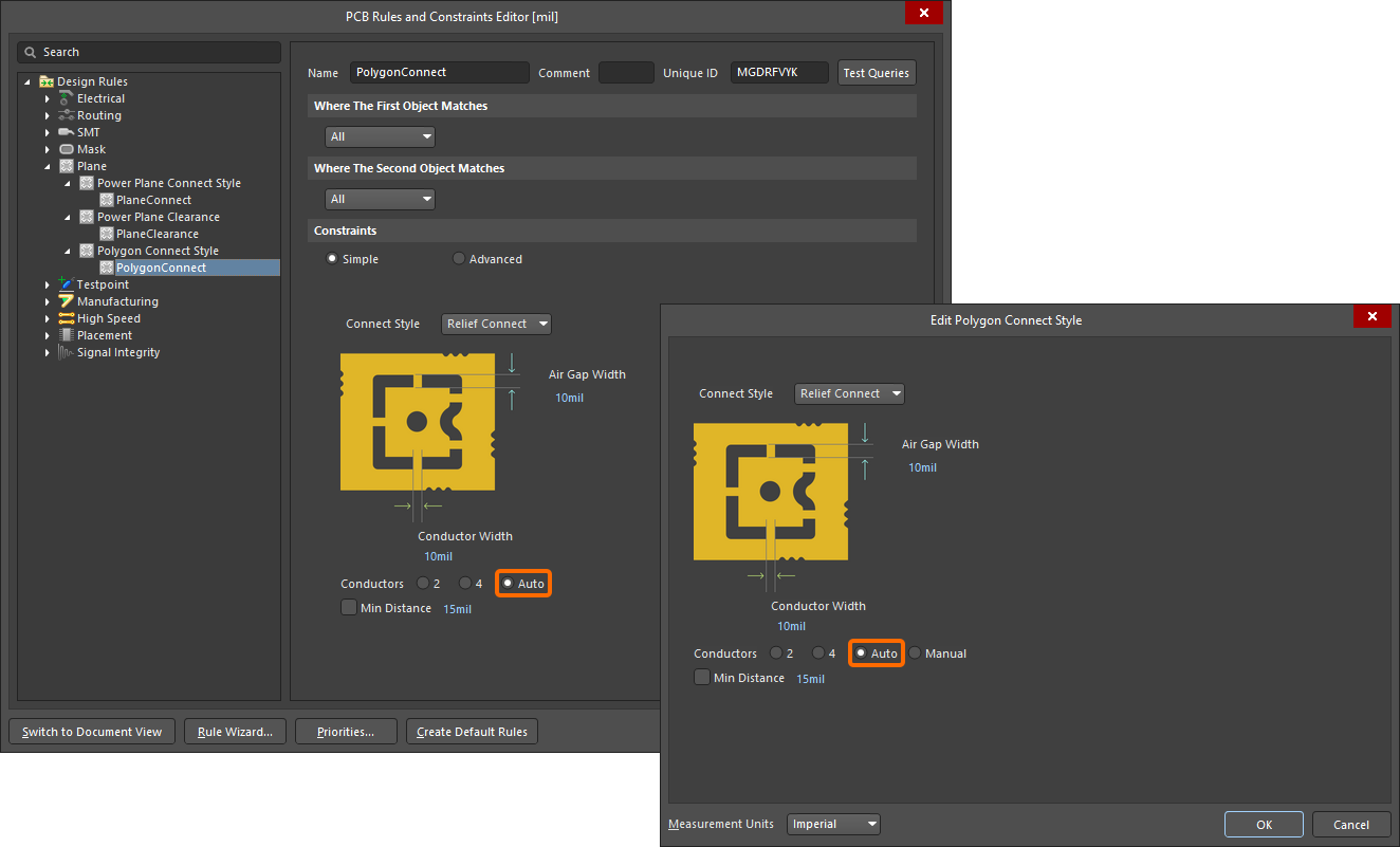
You now have the ability to manually define thermal relief for pads (both regular and custom shaped) by precisely specifying the connection points where the spikes need to connect. Manually-defined thermal relief connections are supported across all pad stack types (Simple, Top-Middle-Bottom, and Full Stack), with the ability to craft connection points as needed for different layers in Full Stack mode. The points themselves can be edited and defined graphically directly within the PCB design space.
To manually define thermal relief connection points, enable the Thermal Relief option in the pad properties, then use the commands in the Pad Actions right-click menu or click the Edit Points button in the Properties panel. After clicking the Edit Points button, you can use Ctrl+Click to graphically add a spoke at any point along the pad shape without invoking the command from the right-click menu. When adding, editing or removing connection points, they are presented as white crosshairs on the pad edge.
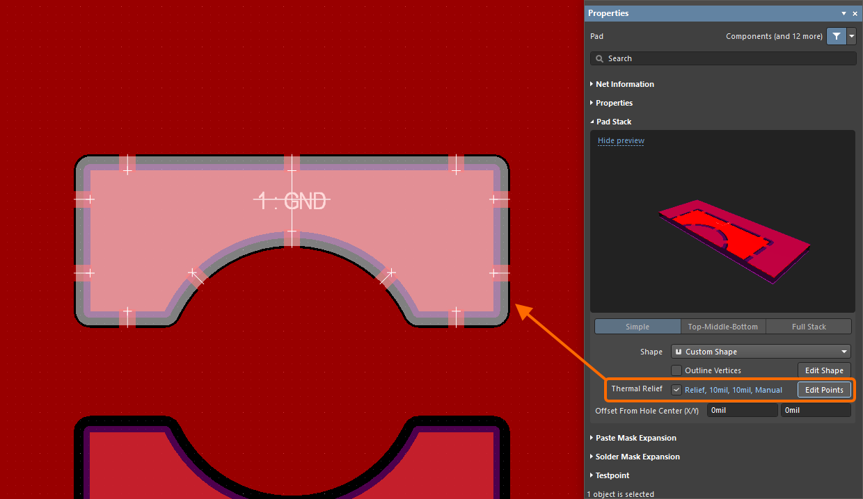
An example of a simple pad with custom thermal relief defined
When thermal relief is manually defined for a pad, it will be denoted by the Manual option in the Properties panel and the Edit Polygon Connect Style dialog that is now accessed by clicking the link in the Thermal Relief field in the Properties panel. If required, you can also choose the minimal distance between the conductors by enabling the Min Distance checkbox and entering an appropriate value.
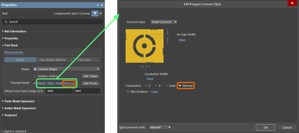
The Xpedition Importer supports importing custom thermal reliefs defined in an Xpedition™ board design. In addition, where a predefined ‘8-leg’ (8-spoke) thermal relief is defined in Xpedition, this will also be imported as a custom thermal relief. Note that Xpedition’s support for the custom rotation of spikes is not supported when imported into Altium Designer.
When opening a document with defined custom thermal relief connections in a previous version of Altium Designer, you will get a warning that this feature is not supported, and, in addition, such defined connections will revert to the standard 4-spoke connections once an associated polygon is repoured.
This feature is in Open Beta and is available when the
PCB.CustomThermalRelief option is enabled in the
Advanced Settings dialog.
Preserve Route Path During Retrace
Added a Preserve route path option to the Gloss And Retrace panel that enables you to preserve the exact trace geometry during Retrace.

When this option is enabled, the Retrace algorithms will not modify the centerline of the trace. Tracks may change width and be split into segments of different widths, but the trajectory will not be changed.
- This option will narrow down a track to avoid a DRC violation, while, with this option disabled, it is possible to shift a trace a bit.
- This option will not remove defects that existed before retrace or that were created by widening the trace.
- This option works only for single-ended traces because preserving the path for differential pairs is impossible without breaking the pair. When retracing a diff pair, its path will be changed if needed, regardless of the state of the option.
Harness Design Improvements
Added New Harness Covering Object
A new Harness Covering object has been added that can be placed over a Harness Bundle on a Layout Drawing document (*.LdrDoc) and can be used to cover in-line components, etc. The length of a harness covering can be graphically modified in the design space during or after placement to specify the start/end gap to the connector. Harness Coverings are available for placement from the Place menu and the Active Bar.
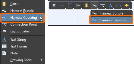
Use one of the placement methods to begin the placement of a Harness Covering. When the cursor is over a valid Harness Bundle object, an orange dot will appear in the design space, which signifies that the Harness Covering can be placed. (A gray dot signifies that a harness covering cannot be placed at that specific place.) Click the orange dot where you want the cover to begin, then move the cursor along the bundle to the point you want the cover to end, then click again. An orange dot appears at the endpoint and the Harness Covering is placed. Harness Coverings can overlap one another, as demonstrated in the video below. Use the Harness Covering mode of the Properties panel to configure the properties of the harness covering.
Layout Label Enhancements
Multi-line text for a Layout Label is now supported. When defining the label's text in the Text field of the Properties panel in its Layout Label mode, use Ctrl+Enter or Shift+Enter to add a new line of text. Enable Show only first line to display only the first line of the Text field in the design space. The Layout Label text can also now be aligned according to your needs using the Alignment controls. Scroll through the below images to see the new features at work.
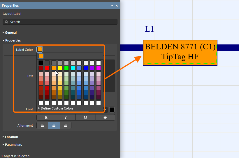
The background color of the label can now be defined in order to distinguish the label from other primitives. Click the color box associated with Label Color, then select the desired color from the pop-up options.
Parameters Added to Connection Points and Layout Labels
Parameters and their values can now be added to Connection Points and Layout Labels that are placed on a Layout Drawing (*.LdrDoc). This allows you to specify, for example, a length parameter for a heat shrink. Click Parameter from the Add drop-down to add a parameter, then configure the name, value, visibility, etc.
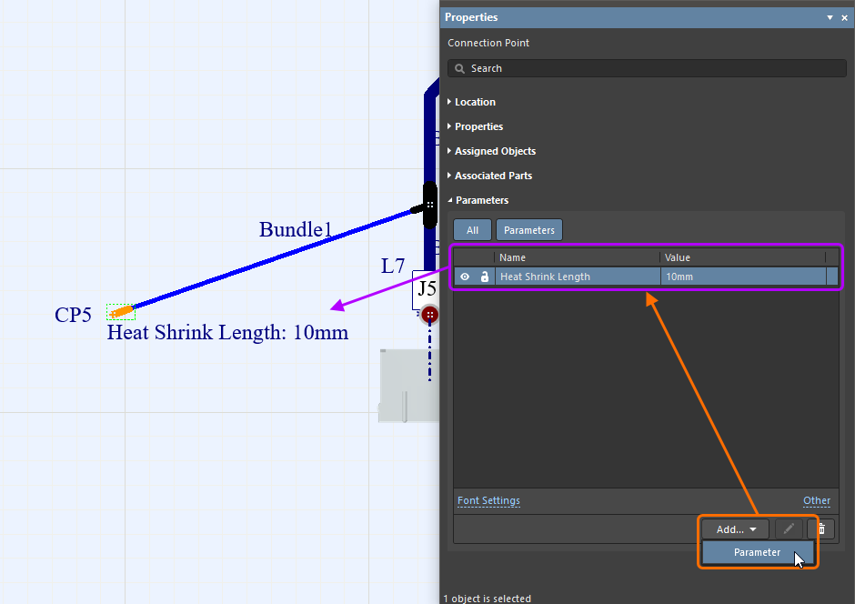
Parameters can now be added to Connection Points and Layout Labels. An example of a parameter added to a Connection Point is shown here. Hover the cursor over the image to see parameters added to a Layout Label.
Data Management Improvements
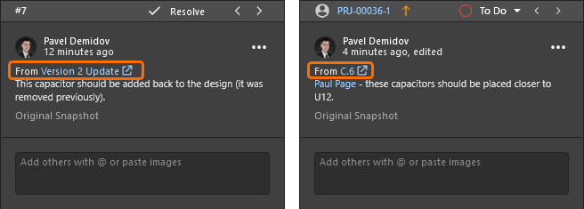
Commit tags and release revision IDs are now displayed when viewing the applicable comments/tasks in both the Comments and Tasks panel and the commenting dialog in Altium Designer.
- Comments created in the Web Viewer when reviewing the design snapshot of a tagged commit will include the associated tag name. Click the tag name link to open the related commit snapshot in the Web Viewer.
- Comments created in the Web Viewer when reviewing a specific release will include the release revision ID. Click the release revision ID link to open the Manufacturing Portal for this release.
Ability to Attach Images to General Tasks
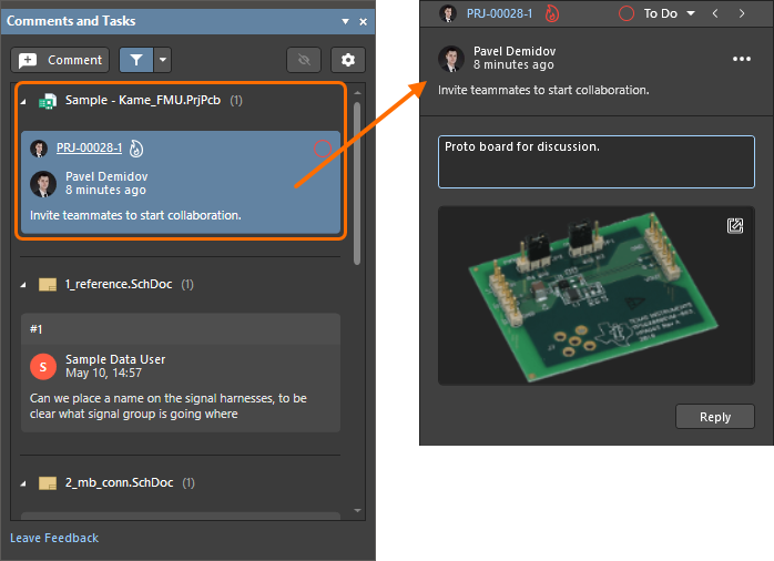
It is now possible to add a comment with an image to a General Task. Click the entry for a General Task in the Comments and Tasks panel to access its commenting dialog. When adding a comment to the task, paste a copied image as you would for a regular comment/task (using the Ctrl+V shortcut or the right-click menu's Paste command).
Circuit Simulation Improvements
Interactive Probes
To assist in exploring simulation results, the concept of interactive probes has been implemented in this release. When the Interactive Mode option is enabled in the Preparation region of the Simulation Dashboard panel, any changes to probes in the design (adding and removing probes, enabling and disabling probes, moving a probe to a different net, changing probe color) will be immediately reflected in the .sdf document.
Demonstration of the interactive probes feature
Note that after enabling the Interactive Mode option, the simulation should be re-run for the feature to work.
Enabling the Interactive Mode option may affect simulation performance and the size of the .sdf document.
This feature is in Open Beta and is available when the
Simulation.InteractiveProbes option is enabled in the
Advanced Settings dialog.
Added PSpice Primitives
The following support has been added:
- Random access read-write memory (RAM) PSpice digital primitive and its URAM timing model.
- Multi-bit D/A converter PSpice digital primitive and its UDAC timing model.
- Bidirectional transfer gate PSpice digital primitives: N-channel bidirectional transfer gate (NBTG) and P-channel bidirectional transfer gate (PBTG).
Altium Designer 23.4
Released: 14 April 2023 – Version 23.4.1 (build 23)
Release Notes for Altium Designer Version 23.4
Key HighlightsExpandCollapse
Harness Design Improvements
Added Fixed Aspect Ratio for Cable/Shield/Twist Objects
To remove the possibility of graphical misrepresentation, harness cables, twists, and shields now have fixed aspect ratios automatically when placing or editing those objects on a Harness Wiring Diagram (*.WirDoc). Also, to avoid transforming these objects into a dot, their minimum size is now determined by the document's current snap grid value.
Live Trace for Wires
When placing a wire in the Wiring Diagram, the netlines now track/refresh 'live,' showing you where to wire in real-time. Previously, the netlines were refreshed only after wire placement was completed. The new live tracing gives a better view of where the wiring is going.
Demonstration of the live trace feature.
Display 3D Model for Connection Point's Associated Part
With this release, a 3D model can be displayed for an associated part of a connection point. In the Connection Point mode of the Properties panel, select Physical Model in the Properties region, then use the Associated Part drop-down in the Views region to select the required associated part. The model will be generated and displayed in the Layout Drawing. Use the options in the Views region to configure the display of the model.
Improved Connection Point Selection
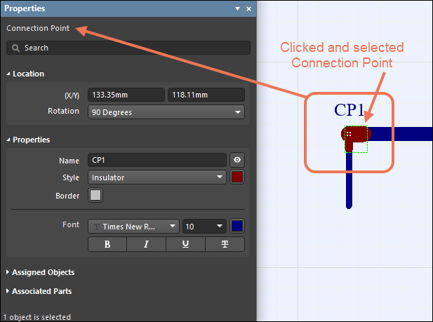
When clicking on a Connection Point in a Layout Drawing linked with a bundle, now only the Connection Point is selected rather than the bundle.
Display Wireframe View for 3D Models
To more precisely display 3D models, a new Style control has been added to the Harness Component mode of the Properties panel. You can now choose to display a model as a wireframe view (Wireframe) or display it shaded with no lines (Solid). The Style control is in the Model region of the panel under Views.
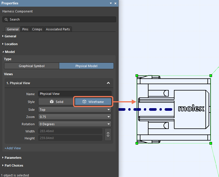 Roll the mouse over the image to see the model using the Solid display Style.
Callouts for Connectors and Connection Points
In a Harness Manufacturing Drawing, a callout associated with a connector or a connection point now displays all BOM item position numbers for its associated parts.
An example of showing BOM item position numbers for associated parts of a connector is shown below.
Circuit Simulation Improvements
Added Support for Output Values in AC Analysis for Controlled Sources and Variable Passives
Output voltage, power and current are now supported in AC Analysis for the following components:
| VCVS |
VCCS |
CCVS |
CCCS |
| VCVS_Table |
VCCS_Table |
CCVS_Table |
CCCS_Table |
| VCVS_Poly |
VCCS_Poly |
CCVS_Poly |
CCCS_Poly |
| VCVS_Expr |
VCCS_Expr |
CCVS_Expr |
CCCS_Expr |
Also, these output values are now supported for variable passives.
Added PSpice Primitives
The following support has been added:
- Added support for the read-only memory (ROM) PSpice digital primitive and its UROM timing model.
- Added support for the multi-bit A/D converter (ADC) PSpice digital primitive and its UADC timing model.
Features Made Fully Public in Altium Designer 23.4
The following features have been taken out of Open Beta and have transitioned to Public in this release:
Altium Designer 23.3
Released: 16 March 2023 – Version 23.3.1 (build 30)
Release Notes for Altium Designer Version 23.3
Key HighlightsExpandCollapse
Schematic Capture Improvements
Automatic Refresh of an ActiveBOM Document
When editing and saving to the connected Workspace components that are used in a project, the ActiveBOM document of the project now refreshes automatically. The Revision Status column will show the Out of date status for changed components, which allows you to immediately see which components should be updated to their latest revisions.
Harness Design Improvements
New Functions on the Crimps Tab of the Properties Panel
To create a more time-saving user interface, copy and paste functions have been added to the Crimps tab of the Properties panel. Select a pin, then use the standard Ctrl+C and Ctrl+V shortcut keys to copy and paste the data to another pin. Multi-selection is also allowed by selecting more than one pin and then using the aforementioned copy and paste shortcut keys.
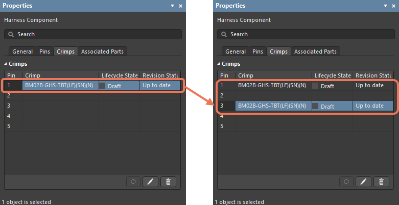
Ctrl+A (select all) and Ctrl+X (cut) functions have also been added to the Crimps tab.
The Delete key on the keyboard can now be used to delete selected crimps using either single or multiple selection.
Free Move of Additional Physical Views
When additional physical views are added for a component on a layout drawing, they can be moved independently using the drag-and-drop action.
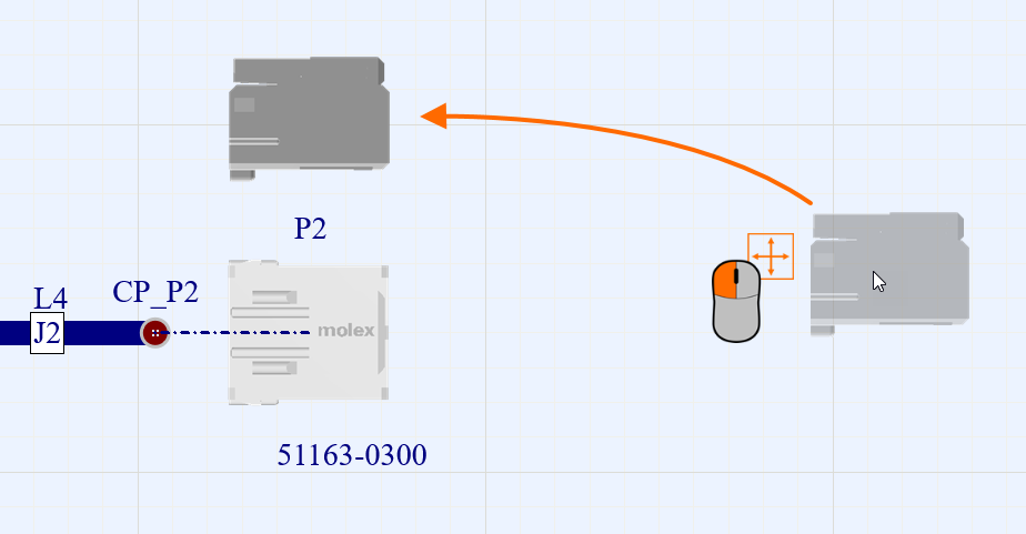
Drag and drop additional physical views of a component to set the view arrangement as required.
'Any Angle' as Default Harness Bundle Placement Mode
Since it is the preferred style for most users, the default placement mode is now 'Any Angle' in the Layout Drawing document when placing a Harness Bundle. During the current session, if a different placement mode is chosen using Shift+Spacebar, the last style used will be the default placement mode.
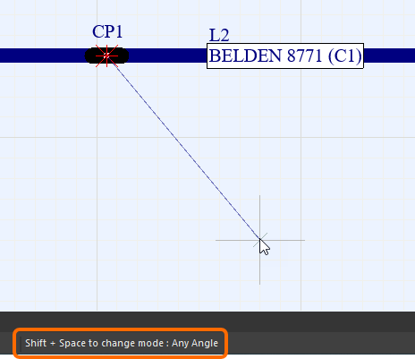
Warning When Assigning an Already Used Object
When an object is assigned to a connection point on a layout drawing, a warning text and icon will display in the Add Assigned Objects dialog (the dialog was previously named Add Connectors). To assist in choosing required objects, the Add Assigned Objects dialog now includes the Current Assignment column that lists the connection points to which an object is currently assigned and the Show only unassigned objects option that allows you to filter out the objects that are already assigned to other connection points.
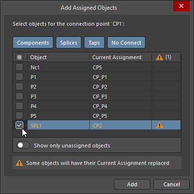
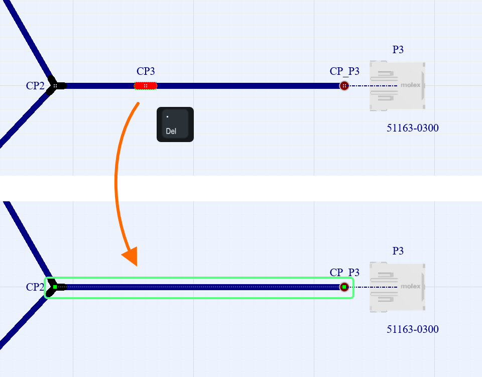
Merging of Bundles When Connection Point is Deleted
When a connection point that splits a bundle on a layout drawing in two is removed, the two bundles are now automatically merged into a single bundle object.
Displaying Graph of Connected Components
In order to assist in understanding the connectivity of components in the layout drawing document, the connectivity graph feature has been implemented for harness designs in this release. When the Connective Graph option is enabled on the System – Navigation page of the Preferences dialog, press the Alt+Click shortcut keys on a component to display the connectivity graph in the design space.
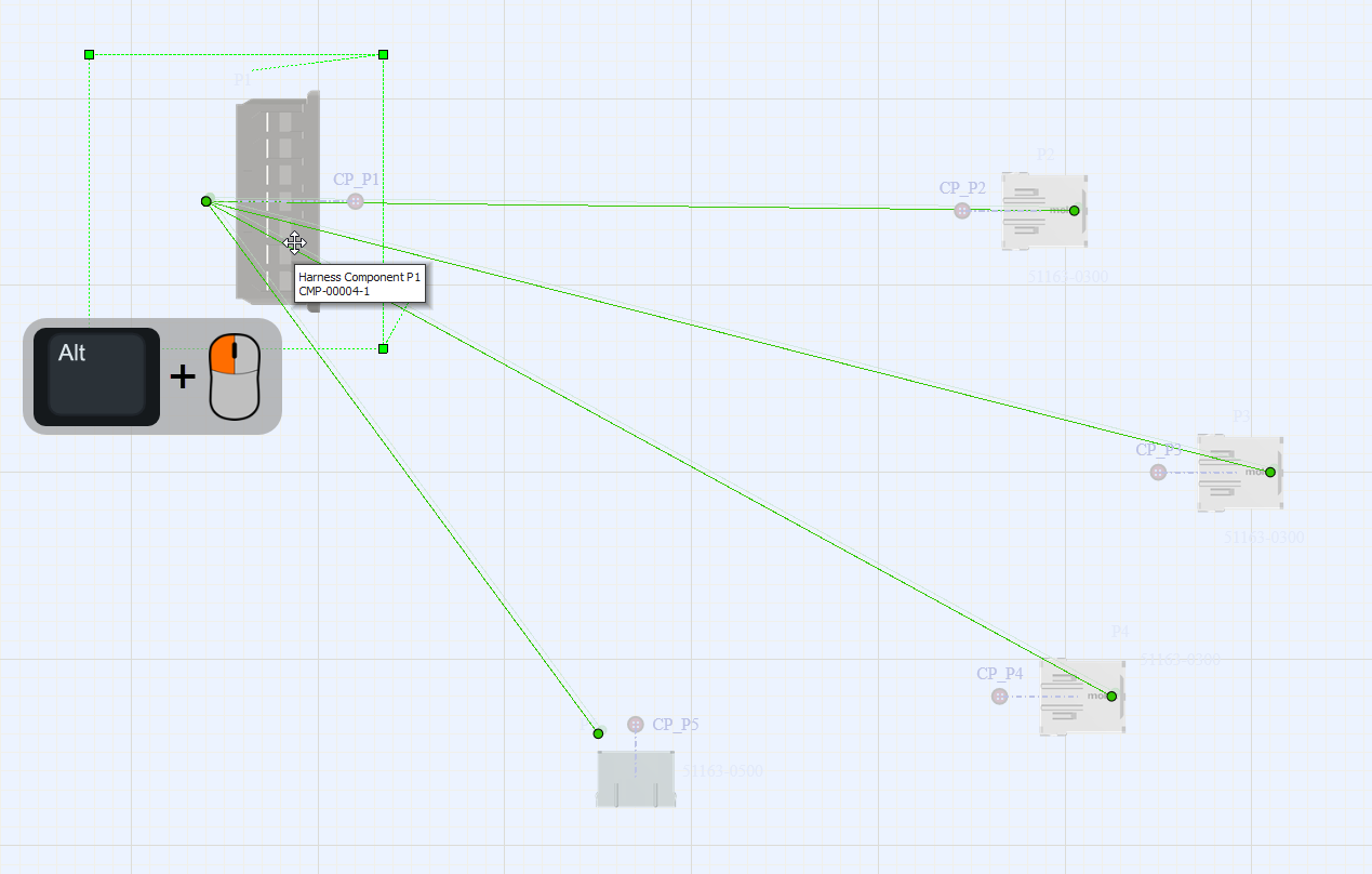
Use the connectivity graph to better understand the component connectivity in a harness layout drawing.
Use the Shift+C shortcut or the Clear Filter command from the right-click menu to clear the graph.
Added Scale Property for the Wiring Diagram View and Layout Drawing View
When a Wiring Diagram View or a Layout Drawing View placed in a harness manufacturing drawing is selected, the Properties panel now includes the Scale region where you can choose a standard scale value or set a custom value.
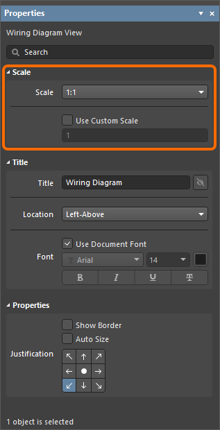
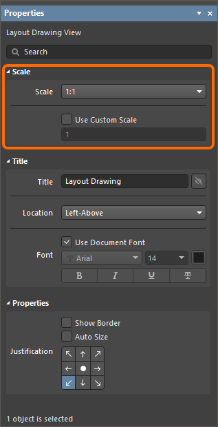
The Scale region of the Properties panel in the Wiring Diagram View or Layout Drawing View mode
Data Management Improvements
Added Workspace-side Project Parameter Support to Draftsman and ActiveBOM
Workspace-side project parameters (those that appear on the Parameters tab of the Project Options dialog with a blue icon:  ) are now supported in Draftsman documents and BOM reports.
- In a Draftsman document, use a special string referencing a Workspace-side project parameter in a Text, Note, or Table object to show the value of that parameter.
- In a BOM report template, use a Field statement referencing a Workspace-side project parameter to get the value of that parameter when generating the report using the BOM template. Learn more about Mapping Design Data into the BOM.
Part Choice Revision Control Improvements
When the Part Choices Revision Control is enabled for your connected Altium 365 Workspace, you will see the following changes in the user interface and user experience:
-
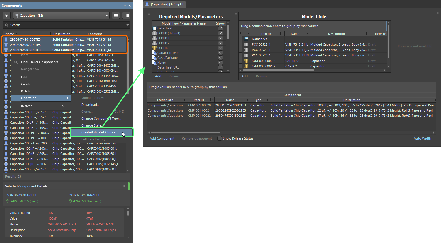
The Create/Edit Part Choices command (previously named Create/Edit PCL) from the Components panel's right-click Operations sub-menu is available now when multiple components are selected in the list. In this case, the Component Editor in the Batch Component Editing mode will open.
-
When comparing component revisions (from the Detailed Item View or the Explorer panel), the comparison of part choices has been enhanced. Comparison is now performed based on the <Manufacturer Name> + <Manufacturer Part Number> combination and the sorting of Part Choices in the Compare component revisions dialog is in descending order by Key: <Rank>_<Manufacturer Name>_<Manufacturer Part Number>.
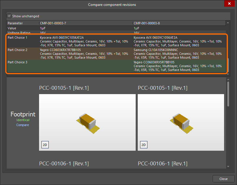
Note that part choice revision control is not supported with the Altium Designer Standard Subscription.
Removed Default File-based Libraries
Beginning with this release, Altera, Lattice, Xilinx, and Simulation folders and Miscellaneous IntLibs (Miscellaneous Connectors.IntLib and Miscellaneous Devices.IntLib) are no longer part of a default installation. Updating to this version of Altium Designer will remove them from the \Library folder.
Circuit Simulation Improvements
Added PSpice Primitives
Added support for the following Programmable Logic Array PSpice digital model primitives:
- PLAND
- PLANDC
- PLNAND
- PLNANDC
- PLNOR
- PLNORC
- PLNXOR
- PLNXORC
- PLOR
- PLORC
- PLXOR
- PLXORC
Added Support for Global Nodes $D_HI, $D_LO, $D_X
Support for digital models that use global nodes $D_HI, $D_LO, and $D_X has been added. These act as if there are digital signal sources connected to them with values 1, 0, and X, respectively.
Added Support for Variable Passives
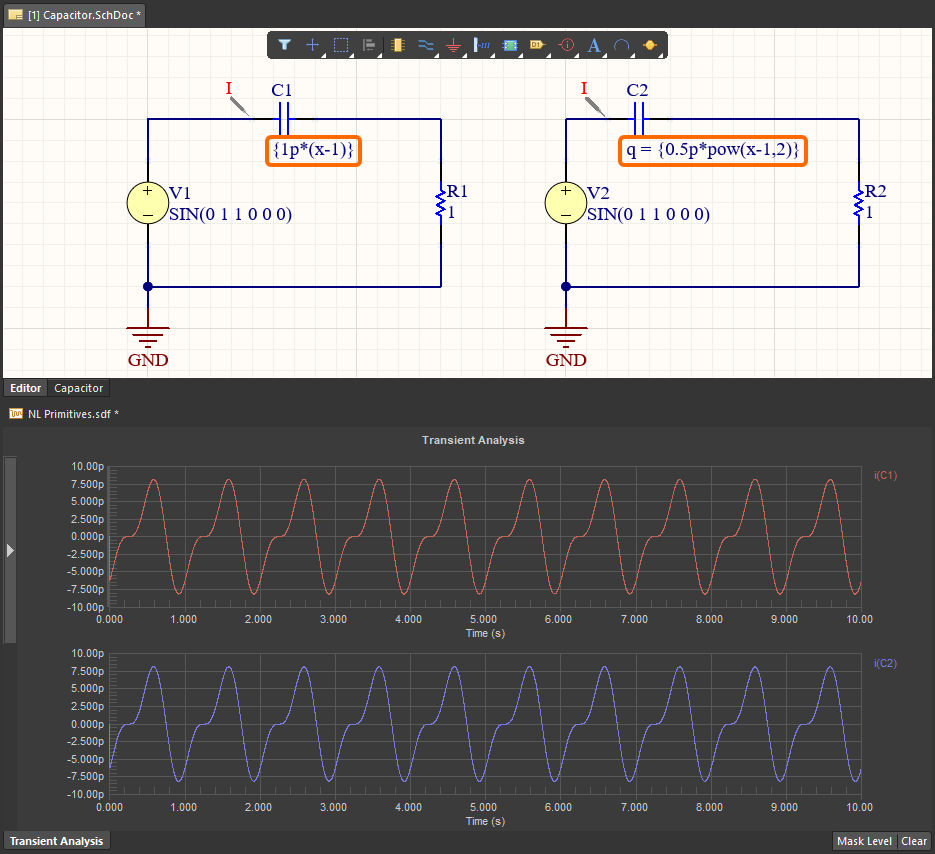
Support for variable resistors, capacitors, and inductors has been added. The value of a passive component can be set as a variable. Use an expression in curly braces as the value of the Value parameter to define resistance for a resistor, the capacitance for a capacitor, or inductance for an inductor. Use the 'q =' or 'flux =' string followed by an expression in curly braces as the value of the Value parameter to define the charge of a capacitor or flux of an inductor.
An example of using variables for capacitors whose capacitance (C1) and charge (C2) depends on the voltage across them is shown below. (The expressions for the capacitance and the charge leads to the same current through the devices, so both resulting waveforms are equal.)
Altium Designer 23.2
Released: 15 February 2023 – Version 23.2.1 (build 34)
Release Notes for Altium Designer Version 23.2
Key HighlightsExpandCollapse
Schematic Capture Improvements
Updating Component Parameters in the Variant Manager
The ability to update the parameters of a component that is used as an alternate part has been added to the Variant Manager. Select the Update Values from Library command from the right-click menu of the Parameter region at the bottom of the Variant Manager or in the Component Parameters region of the Properties panel when the required alternate component is selected in the main grid area to bring any parameter changes made to a library component. Browse to and locate the component in the source library via the Replace dialog and click OK to open the Update Project Variants From Library dialog. Select/deselect the Parameters from Library Component and Variants to Update, then click OK to complete the update process. Note that this updates the parameters only and not the component itself.
Select the Update Values From Library command from the Parameter region or the Properties panel in the Variant Manager and use the subsequent dialogs to update an alternate part's parameters.
Room Generation Disabled by Default
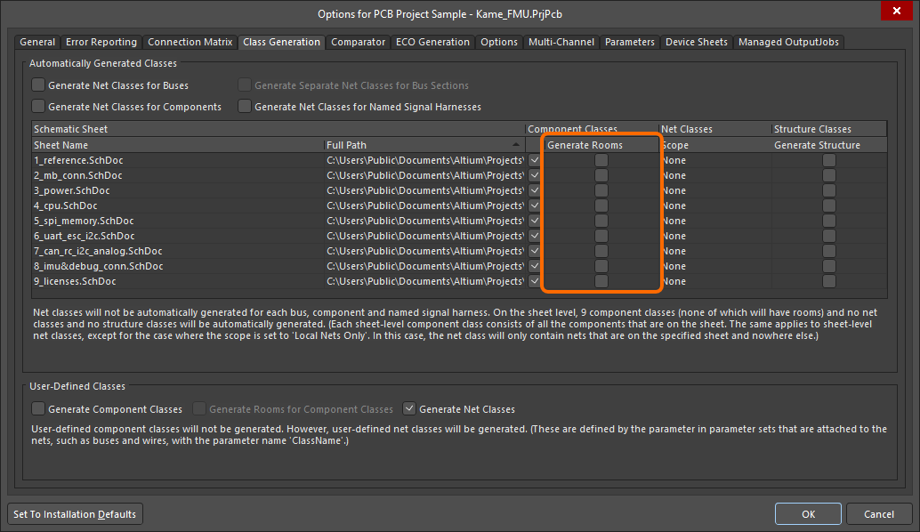
Starting from this release, the Generate Rooms checkboxes on the Class Generation tab of the Project Options dialog are disabled by default for schematic sheets in new PCB design projects. As such, rooms associated with component classes will not be generated on the PCB by default when transferring design data to the PCB.
PCB Design Improvements
Gerber Setup Layer Class Support
The Gerber Setup dialog now includes a Layer Classes section in its Layers to plot list. Using the checkbox for layer classes, you can quickly enable plotting for all the layers that belong to a specific layer class. Default layer classes (Component Layers, Signal Layers, Electrical Layers, and All Layers) and any user-defined layer classes (those defined in the Object Class Explorer dialog) will be listed here.
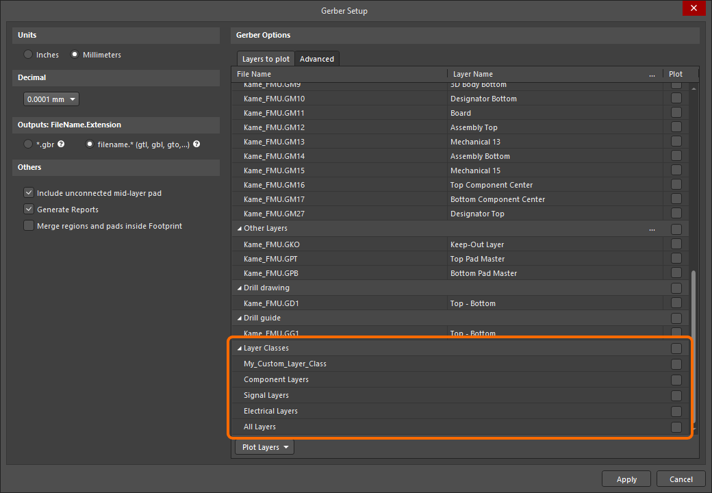
Use the Layer Classes region of the Gerber Setup dialog to quickly enable the plotting of a specific layer class.
Data Management Improvements
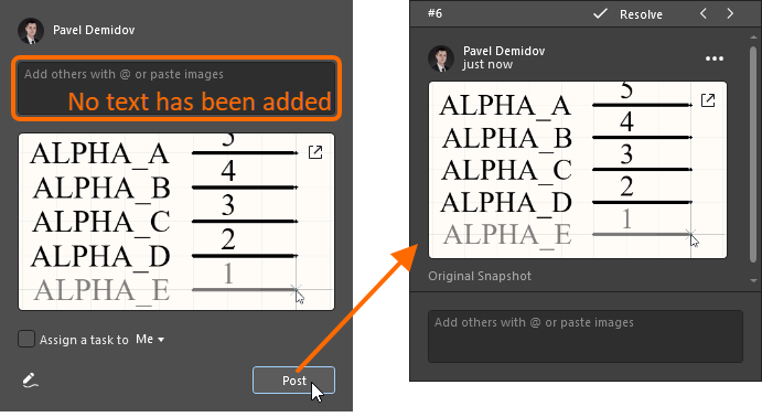
It is now possible to post a comment even when it includes only a pasted image without any text.
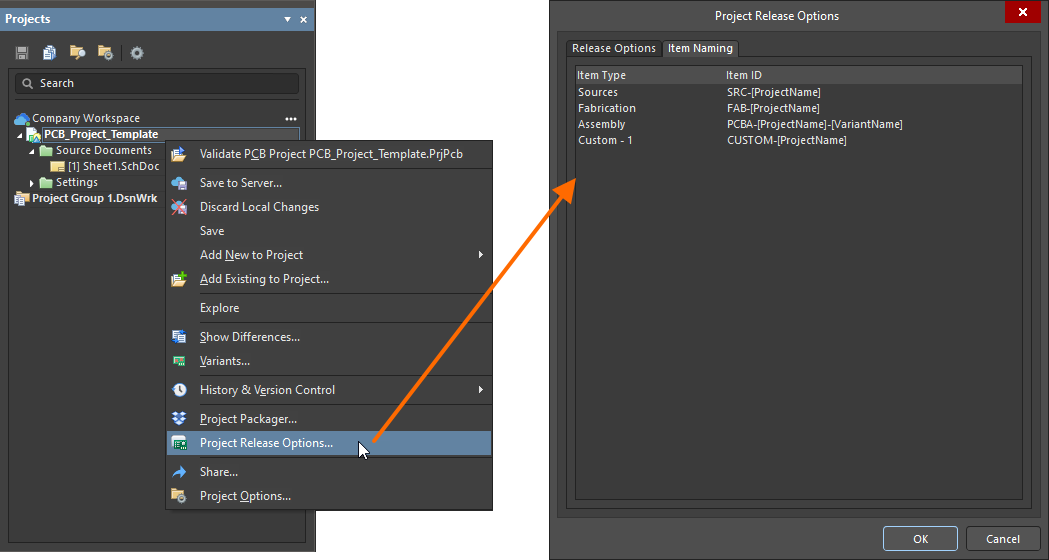
Editing of Item Naming Schemes for Project Templates
It is now possible to access and edit Item Naming schemes for project release target data items when editing a project template saved to the connected Workspace. To do this, open a saved project template from the Workspace, right-click the template's entry in the Projects panel, then select the Project Release Options command. You can configure item naming schemes on the Item Naming tab of the Project Release Options dialog that opens.
Harness Design Improvements
Repeat Crimp Type
A crimp added to a pin of the selected harness component can now be quickly added to all pins of this component. Select the entry of the required crimp then click the Repeat To All button. The selected crimp will be added to all other pins of the component.
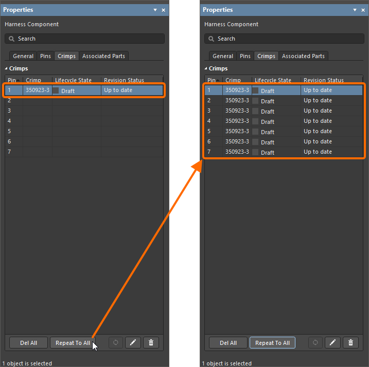
Auto-generate Splice on Wire Junctions
When two wires are connected in a T-type fashion, a splice is now placed automatically at the location of the T-junction.

A splice is automatically placed where a T-junction occurs.
Updated Wiring Diagram Icons
Several icons for placing primitives on a wiring diagram have been updated to represent the primitives better. Icons have been updated on the Place menu and right-click menu, and the Active Bar.
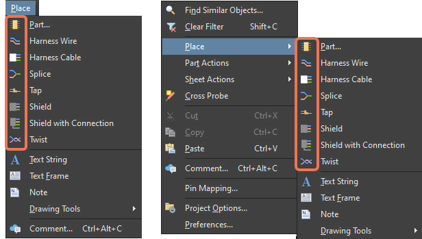
Remove Splice from a Connection Point after Assigning to Another
To avoid assigning a splice to more than one connection point, a splice is now removed automatically from a connection point if it is assigned to another connection point.
Demonstration of splice assignment auto-removal.
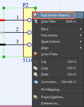
Added Ability to Find Similar Objects
The Find Similar Objects command has been added to the right-click menu of a primitive in harness documents (wiring diagrams and layout drawings). The command functions the same as in schematic documents.
Resetting Component Designators on Paste
When pasting cut/copied harness components on a Wiring Diagram or Layout Drawing document, designators of pasted components now respect the Reset Parts Designators On Paste option from the Schematic - Graphical Editing page of the Preferences dialog. When components are pasted, the numerical part of their designators will reset to "?" when the option is enabled.
Importer/Exporter Improvements
Exported AutoCAD Layer Names
Layer names that are defined in the Layer Stack Manager are now the names that are used in AutoCAD exports.
Circuit Simulation Improvements
Added PSpice Primitives
Added support for the following PSpice digital model primitives:
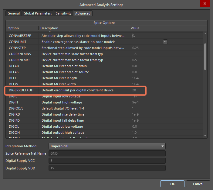
Added DIGERRDEFAULT Option
Simulation option DIGERRDEFAULT has been added to control the amount of reported constraint violations in digital primitives. The new option can be found on the Advanced tab of the Advanced Analysis Settings dialog (click Settings in the Analysis Setup & Run drop-down of the Simulation Dashboard panel).
Features Made Fully Public in Altium Designer 23.2
The following feature has been taken out of Open Beta and has transitioned to Public in this release:
Altium Designer 23.1
Released: 17 January 2023 – Version 23.1.1 (build 15)
Release Notes for Altium Designer Version 23.1
Key HighlightsExpandCollapse
Schematic Capture Improvements
Compiled Names of Power Ports
The Net Labels option in the Compiled Names Expansion region of the Schematic - Compiler page of the Preferences dialog now determines the name for a Power Port object on the compiled (physical) tab of a schematic document.
An example of strict hierarchical multi-channel design schematics that includes net labels and power ports. Note that when viewing compiled tabs of the schematic sheet, the power ports display the physical name in the same way as the net label does.
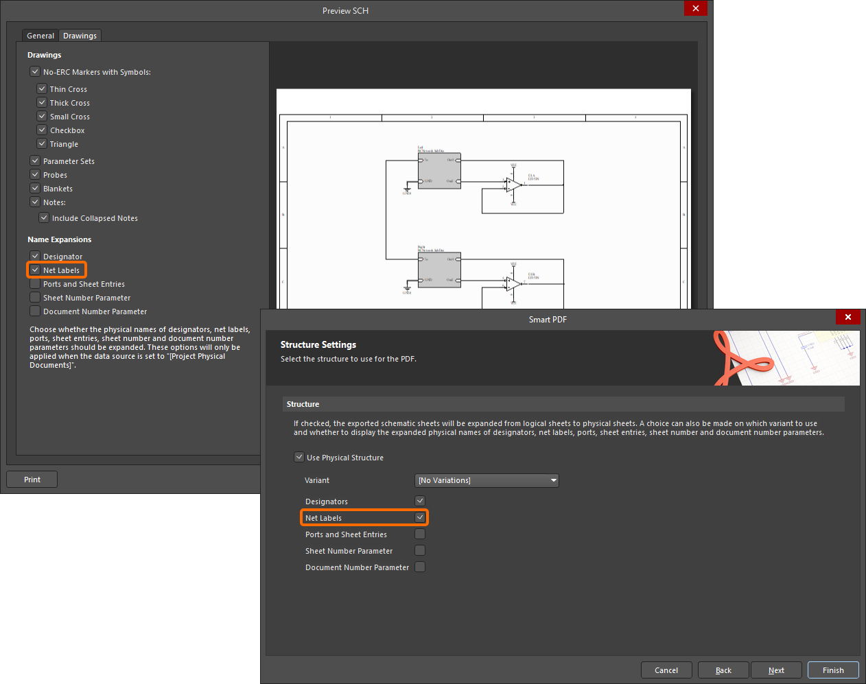
The Net Labels option in the Print dialog (when accessed from an Outjob file for a schematic print output with the [Project Physical Documents] option selected as the output's data source) and on the Structure Settings page of the Smart PDF Wizard also defines how the power ports will be shown in the schematic outputs.
PCB Design Improvements
Load a Stored View Configuration File
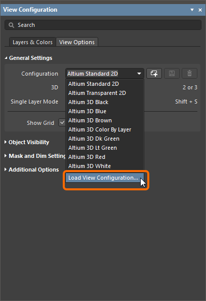
Added the ability to load a stored view configuration file from the View Options tab of the View Configuration panel. Use the Load View Configuration option from the Configuration drop-down to browse to and select the required view configuration file.
Rename the Gerber Board Outline File
You can now rename the Gerber Board Outline type file in the Gerber Setup and Gerber X2 Setup dialogs.

Improved Callstack Crash Report Content
This feature uses an enhanced method to collect callstack crash reports.
Data Management Improvements
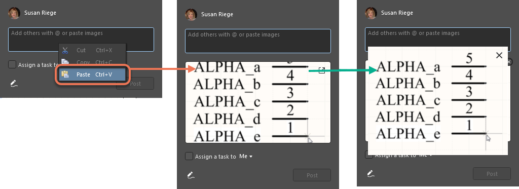
This update adds the ability to attach images to your comments. As is said, a picture is worth a thousand words so attaching images will help explain your ideas to coworkers or highlight the location of an issue. You can add an image to a comment by first copying the image from an Explorer window or a web browser page by right-clicking on the image, which copies the image to the clipboard. To attach the image, use right-click Paste (or the Ctrl+V shortcut) in the comment itself (in the field that states "Add others with @ or paste images").
Each image can be a maximum of 2MB. After it is pasted into the comment, click the image to display the full image, as shown in the image on the right.
Added the ability to export the Project History from the Reports menu to a PDF. After choosing Reports » Project History from the main menus, the Project History Report Configuration dialog opens in which you can set the Period for which the report should be exported: either the entire project history or from/to a specific (or the latest) project release. Click Export then enter a name for the exported PDF in the Explorer window that opens then click Save. The PDF report opens in a web browser.

Note that the project history report export functionality is not supported with the Altium Designer Standard Subscription.
Harness Design Improvements
Crimps in Wiring Diagram
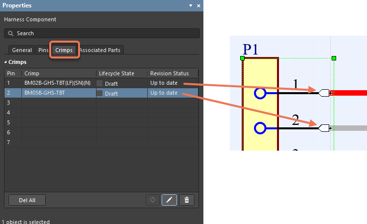
Crimps can now be used on the Wiring Diagram (*.WirDoc) as was previously available in the Layout Drawing. The Crimps tab of the Harness Component mode of the Properties panel can be used to add and edit crimps using the  icon. A crimp is denoted by a
  in the design space as shown below.
Twist and Shield Parameters
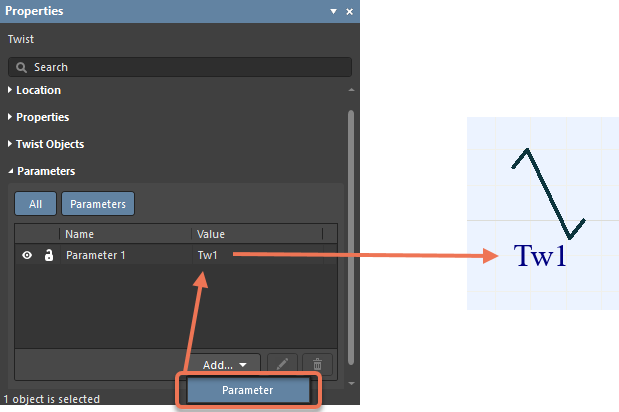
Parameters have been added to Twist and Shield objects in a Wiring Diagram document (*.WirDoc). During or after placement of a twist or shield, click Parameter in the Add drop-down of the Properties panel, then update the desired visibility, parameter name and value. An example of a twist object is shown in the below image.
Quickly Add Connection Point Objects
The ability to add connection point objects to the Layout Drawing (*.LdrDoc) has been added. This allows you to add multiple objects to a connection point with one action. In the Connection Point mode of the Properties panel, click Add in the Connectors region to open the Add Connectors dialog. In the dialog, enable the connectors for the connection point. To enable all in the list, enable the checkbox next to Connector.

Additional Physical Views
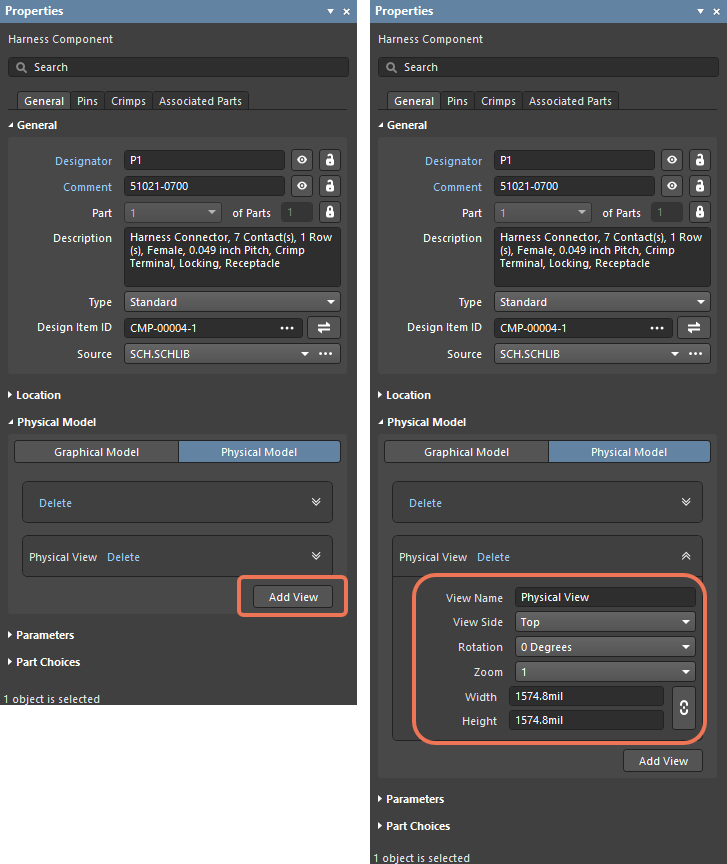
With this release, you can add multiple 3D physical model views for a connector in a Harness Layout Drawing (*.LdrDoc) document. In the Physical Model region of the Harness Component mode of the Properties panel, select Physical Model then click Add View. A physical view will be added. You can see and update the view's parameters by clicking the corresponding  icon.
icon.
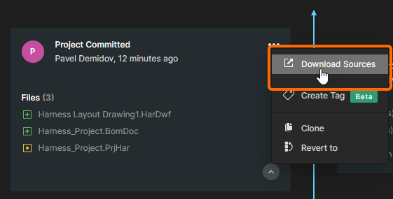
Added Download Sources to Project History
You can now download and open a specific revision of a project (in the Projects panel) using the Download Sources command. In a Project History file (<ProjectName> History), click  then select Download Sources. The downloaded revision opens in the Projects panel. Note that this revision is read-only, i.e. you can view but not edit it in any way.
Ability to Save as ASCII
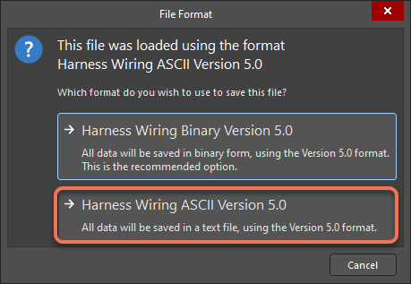
You can now save Harness Design Wiring Diagram (*.WirDoc) and Layout Drawing (*.LdrDoc) documents in ASCII format, which can be beneficial when sharing. Use the File » Save As command and select Harness Wiring ascii (*.WirDoc) or Harness Layout ascii (*.LdrDoc) from the Save as type drop-down in the Save As dialog that opens.
When saving an ASCII Wiring Diagram or Layout Drawing document using the File » Save command, the File Format dialog will open alerting you that the ASCII format is used. Choose the ASCII Version (highlighted in the below image) in the dialog to keep using this format.
Added Autosize and Justification
Added Auto Size and Justification properties to the Properties panel for the Wiring Diagram View and Layout Drawing View objects in a Harness Project Draftsman document (*.HarDwf).
When Auto Size is enabled, the Wiring Diagram View automatically adjusts its size to remove empty space at the borders. Select the Justification by clicking on an arrow that corresponds with the desired justification or the circle to center. The chosen option for Justification defines the point relative to which the position of the view is changed if its size is updated.
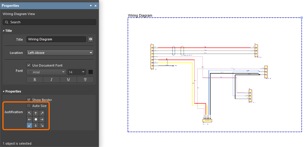
Example of a Wiring Diagram View with the Auto Size option enabled and Justification set to bottom-left. Hover the cursor over the image to see the view with the Auto Size option disabled - note that the location of the view is changed relative to its bottom-left corner.
Multi-board Improvements
Allow Pin Connection to More Than One Pin
When configuring a connection of the Harness type on a Multi-board schematic document (*.MbsDoc), you can now connect a pin from one PCB connector to more than one pin on the same target PCB connector.
![An example of the connection configuration of a harness connection in a Multi-board schematic. Note that the same pin of the source connector (H_1-Entry_1[1]) is connected to multiple pins of the same target connector. An example of the connection configuration of a harness connection in a Multi-board schematic. Note that the same pin of the source connector (H_1-Entry_1[1]) is connected to multiple pins of the same target connector.](https://www.altium.com/documentation/sites/default/files/wiki_attachments/320598/MBS_ConnectToMultiplePins_AD23_1.png)
An example of the connection configuration of a harness connection in a Multi-board schematic. Note that the same pin of the source connector (H_1-Entry_1[1]) is connected to multiple pins of the same target connector.
Circuit Simulation Enhancements
Inertial Delay
Implemented inertial delay processing for all PSpice digital gates (except DLYLINE).
Added PSpice Primitives
Added support for the following PSpice digital model primitives:
Altimade Enhancements
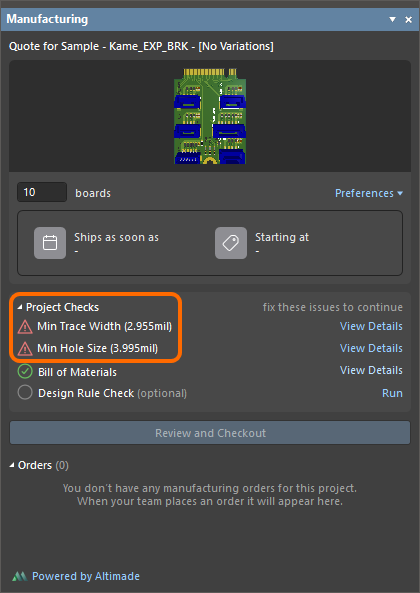
Relaxed Constraints for the Min Trace Width and Min Hole Size
Constraints for the Min Trace Width and Min Hole Size have been relaxed to allow for 3mil and 4mil respectively.
Altium Designer 23.0
Released: 15 December 2022 – Version 23.0.1 (build 38)
Release Notes for Altium Designer Version 23.0
Key HighlightsExpandCollapse
PCB Design Improvements
Silkscreen Preparation
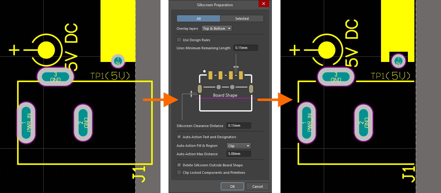
To assist in resolving common Design for Manufacture (DFM) issues faced by having silkscreen overlapping exposed copper, holes and board shape, a dedicated feature for preparing the silkscreen for your boards has been implemented in this release. These issues can now be effectively addressed by:
- automated clipping of silkscreen lines and arcs
- automated clipping or movement of fills and regions
- automated movement of silkscreen text and component designators.
The feature is available in both the PCB footprint editor (for the active footprint) and PCB editor (across all or selected objects on one or both overlay layers) using the Silkscreen Preparation dialog, which is accessed by using the Tools » Silkscreen Preparation command from the main menus.
This feature is in Open Beta and is available when the
PCB.SilkScreenPreparation option is enabled in the
Advanced Settings dialog.
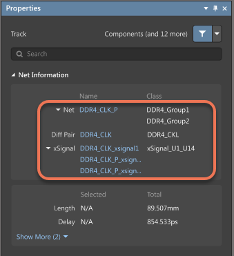
The Net Information region of the Properties panel now displays all nets, differential pairs, and xSignals for the selected primitive. You can expand the sections to view all listed information.
Data Management Improvements
Manage Missing Files
Previously, missing files were removed with a corresponding notification in the Messages panel and the project was marked as modified in the Projects panel. This release includes an enhanced approach to managing files defined within the project file but not found within the project folder. Rather than simply removing references to such files and marking the project as modified, these files are now marked as ‘missing’. They remain defined in the project file and still appear listed in the project’s structure in the Projects panel, but they are now grayed out and have a distinguishing icon.
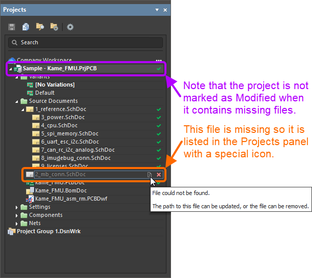
Associated commands are available that give you full control over handling missing documents. Using the right-click menu of a missing file in the Projects panel to remove the selected or all missing files from the project or to update the path to the file (i.e. to replace the missing file with a selected one). For a project that is under version control, you can also revert local modifications to restore a missing file from the project's VCS repository.
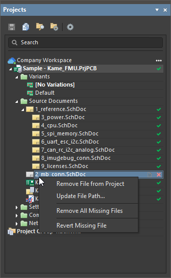
When adding an existing file to the project using the Add Existing to Project command from the project entry's right-click menu and the name and the path of the file being added are the same as the name and the path of a missing file (which is possible when, for example, the missing file was added to the project folder after opening the project in Altium Designer), a confirmation dialog will open asking if you would like to replace the missing file with the selected one.

This feature is in Open Beta and is OFF by default. It is available when the
WSM.ManageMissingFiles option is enabled in the
Advanced Settings dialog.
Creating a Project History Report
A Project History PDF report can now be created for a Workspace project. In the OutputJob file (*.OutJob), right-click on the [Add New Report Output] associated with the Report Outputs entry then choose Project History.

The newly-created Project History output report can then be connected to a PDF output container.
Right-click the created output then select Configure to access the Project History Report Configuration dialog in which you can set the Period for which the report should be exported: either the entire project history or from/to a specific (or the latest) project release.
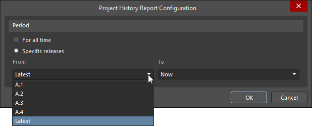
When the report is added, linked to the required PDF output container, and configured as needed, click Generate content or generate output as part of the project release process to export the project history.
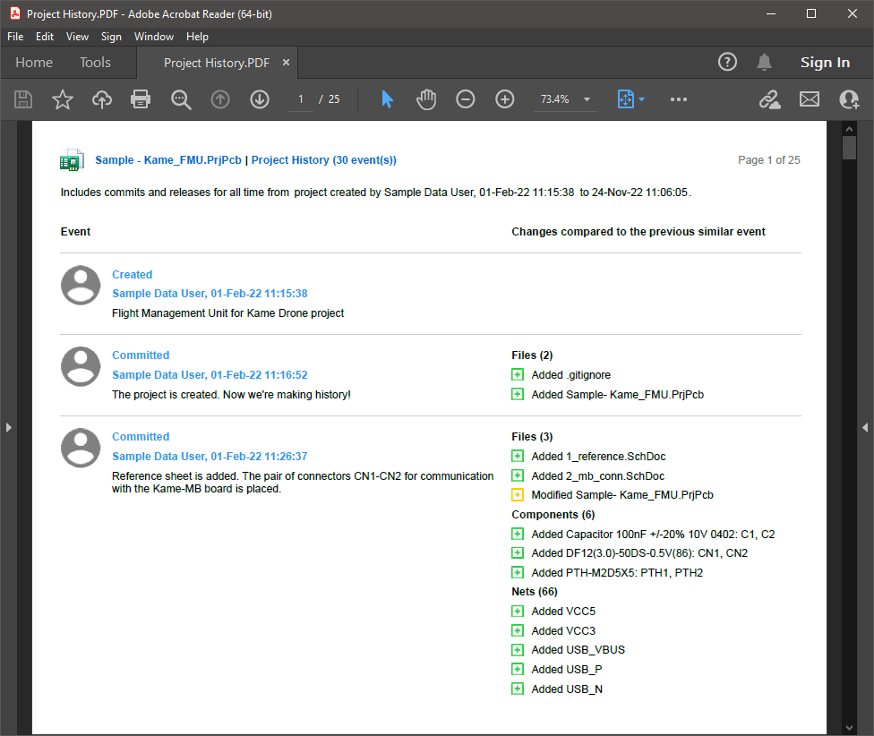
An example of a project history report
Note that the project history report export functionality is not supported with the Altium Designer Standard Subscription.
Support has been added for layer-specific comments on the PCB in 2D. Focusing a comment will auto-switch to the same view the reviewer had (visible layers, active layer, top/bottom view).
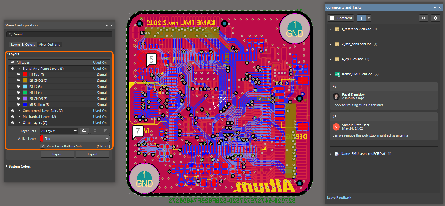
Example of view configuration switch when focusing a comment. Shown here is the view configuration before focusing on a comment: all layers are enabled, Top is the active layer, and the board is shown from the bottom side. Hover the cursor over the image to see the board after focusing on a comment (the same view is applied as it was when the comment was added): Bottom is the only signal layer enabled, Bottom is the active layer, and the board is shown from the top side.
Ability to Delete Workspace Repository
A Workspace repository that appears in the Data Management - Design Repositories page of the Preferences dialog after migrating a project managed by an external VCS to the Altium 365 Workspace VCS can now be deleted if the repository has no reference to a Workspace project.
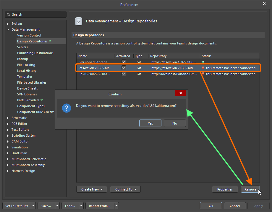
After successful migration of a project from an external VCS to the Workspace VCS, the repository will be removed from the Workspace automatically.
Notes:
- You must be an administrator of the Workspace to be able to delete a repository.
- If a project has been soft deleted (moved to Trash), it must be deleted permanently so the repository referencing it can be removed.
- The Workspace's
Versioned Storage repository cannot be removed.
Harness Design
This release sees the first implementation of the Harness Design capability. This new tool allows new engineers of various types (involved in the Product Design process) to work in Altium Designer. It brings comprehensive harness design support into the same environment as PCB and system design, removing the previous heavy reliance on third-party software.
The Harness Design tool allows you to create a full wiring harness design, from individual pin-to-pin connections to manufacturing documentation. A harness design can be created as a standalone project, or as part of a Multi-board project. In the latter case, the logical connections between PCBs in the Multi-board project are used to define the connectivity within the harness.
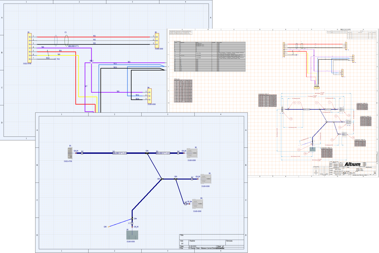
This release includes a sample harness design project (Harness_Demo_Prj.PrjHar), which is associated with a new multi-board demo project (Harness_Demo_MB.PrjMbd), so you can take harnesses for a test drive straight out of the box.
This feature is in Open Beta and is available when the
System.HarnessDesignAvailable option is enabled in the
Advanced Settings dialog. Note that Harness Design functionality is not supported with the Altium Designer Standard Subscription.
ActiveBOM Enhancements
This release includes several enhancements when working with alternative components in ActiveBOM.
Retaining Filters and Values in the Add Alternative Item Dialog
The Add Alternative Item dialog, which is accessed by right-clicking a Workspace component and selecting the Operations » Add Alternative Item command in the context menu now remembers the used filters and values when accessing the dialog for different components of the same type.
Preventing Replacement of an Alternative Component with an Already Used One
When trying to replace an alternate component with one already used as an alternative, a warning dialog appears to alert you.

Confirmation for Removal of an Alternative Group with Alternate Components
When trying to remove a group of alternatives and the components in this group have an alternate component assigned, a warning dialog appears to alert you and asks for confirmation to delete the group.

Circuit Simulation Improvements
High-impedance State
Added the ability to view the high-impedance state for digital waveforms in the SimData editor.

PSpice Enhancements
Support for the following PSpice primitives has been added in this release:
- LOGICEXP
- Digital delay line
- Digital Pullup and Pulldown
- DFF
- JKFF
- DFFDE
- JKFFDE
Also, components for the following PSpice primitives were added to the Simulation Generic Components library:
- Standard gates
- Tristate gates
- Digital stimulus
Features Made Fully Public in Altium Designer 23.0
The following features have been taken out of Open Beta and have transitioned to Public in this release: