PCB Layout Replication
The PCB Layout Replication tool gives you the ability to replicate the layout for repetitive blocks of circuitry in a flat PCB design. As an informal reuse feature, this tool is a perfect fit when you need to quickly replicate placement of a group of components to another group of the same, not-yet-placed components with the same connections.
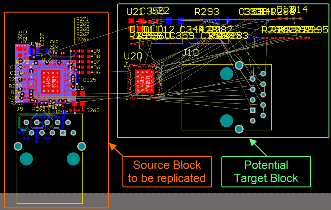
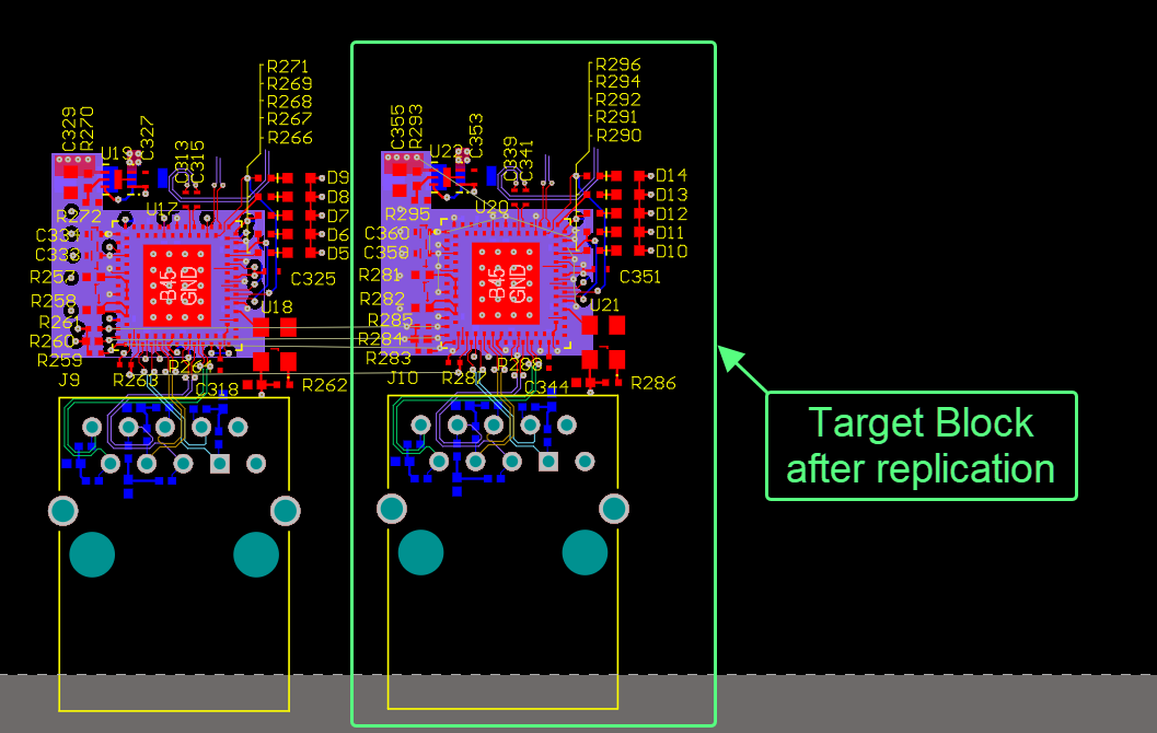
On the PCB document, a fragment of the captured design to be replicated (the Source Block) can be selected, and then that layout can be applied to each fragment of the design that is detected to be a match (Target Blocks). You have full control over which target block(s) to apply replication to and can specify what that replication should include besides component placement (e.g., routing objects).
|
An example of applying the PCB Layout Replication tool. The source block with components placed and routed as required and the components of the potential target block are shown here. The blocks after applying the PCB Layout Replication tool. |
The process of replicating blocks using the tool is the following:
-
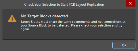
In the PCB document, select the source block of objects to be replicated: components and, optionally, other objects: tracks, arcs, pads, vias, polygons, regions, and/or fills. For the PCB Layout Replication tool to detect target blocks on the PCB, they must have the same components (placed from the same library) and connectivity as the selected source block. Note that objects not included in the selection will not be replicated in target blocks.
-
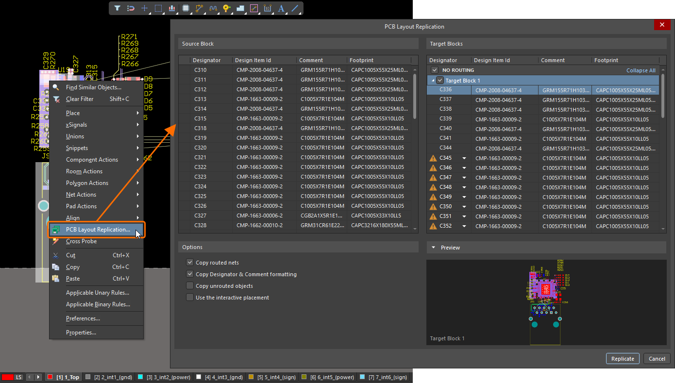
Choose the Tools » PCB Layout Replication command from the main menus (or right-click the selection and choose the PCB Layout Replication command from the context menu). The PCB Layout Replication dialog will open if at least one target block is detected.
-
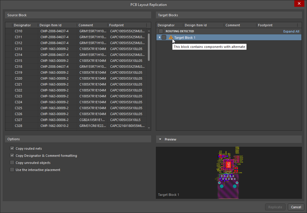
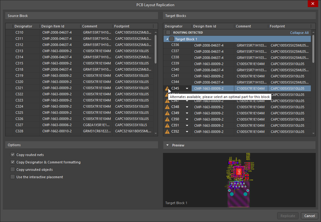
Components of the source block will be listed in the left-hand Source Block region of the PCB Layout Replication dialog, and the detected target block(s) will be listed in the right-hand Target Blocks region of the dialog. Expand/collapse target block entries to show/hide the list of components of the target blocks. Use the checkboxes next to target block entries to select the target blocks to which replication should be applied.
- If no routing is detected in a target block, it will be listed in the NO ROUTING category of the dialog's Target Blocks region. Such target blocks are included in replication by default (their checkboxes are enabled).
- If an existing routing is detected in a target block, this target block will be listed in the ROUTING DETECTED category of the dialog's Target Blocks region. By default, such target blocks are not included in replication (their checkboxes are disabled). If you choose to enable such a target block in replication, note that the existing routing between components will be removed, and if the Copy routed nets option is enabled in the dialog, routing from the source block will be placed. Unrouted objects of the target block will remain as they are.
Use checkboxes at the left of the NO ROUTING and ROUTING DETECTED categories to select/deselect all target blocks in the corresponding category. Use the Expand All / Collapse All control to expand/collapse all target block entries in the corresponding category.
- Use checkboxes in the Options region to configure what replication should include:
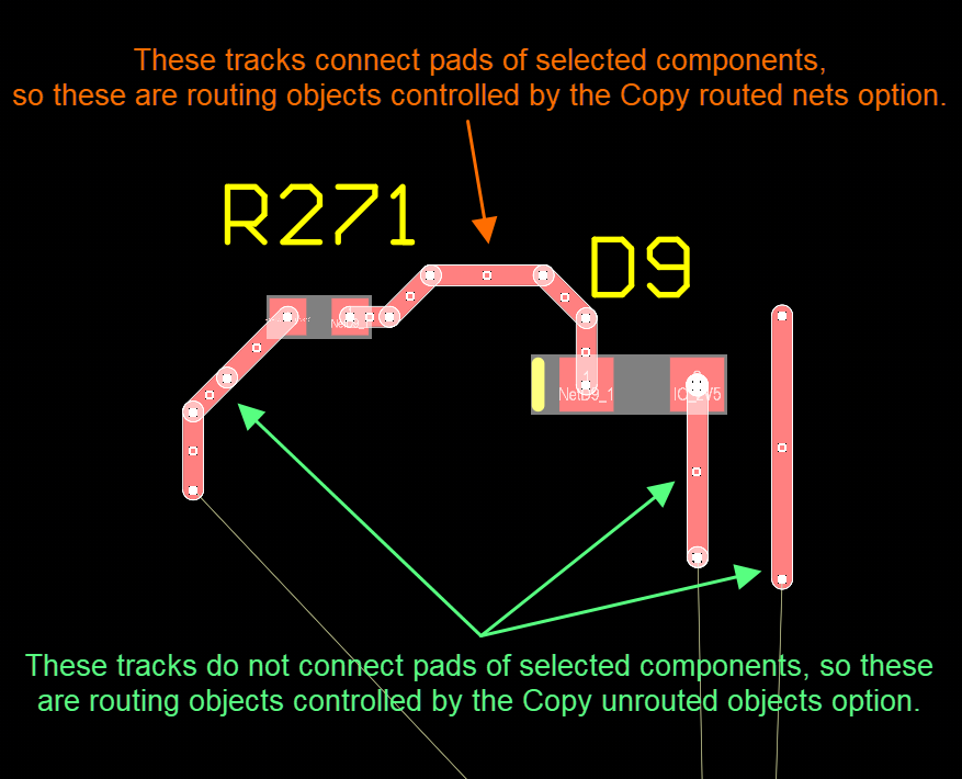
- Copy routed nets – enable this option to replicate copper objects (tracks, arcs, pads, vias, fills, regions, and polygons) connecting components in the source block.
- Copy Designator & Comment formatting – enable this option to apply the formatting of designator and comment strings of components in the source block to those in the target blocks.
-
Copy unrouted objects – enable this option to replicate objects other than routing between components, i.e. copper objects (tracks, arcs, pads, vias, fills, and regions) that do not connect source block components – either routing objects that are connected to only one pad of a component in the source block or routing objects that are not connected to any component pad in the source block.
- Use interactive placement – the state of this option defines how the target blocks will be placed once the Replicate button is clicked in the dialog:
-
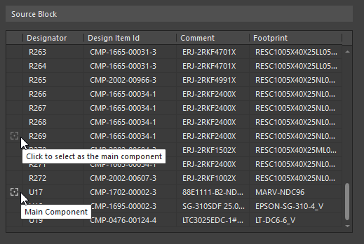
When this option is disabled (default), each target block will be positioned relative to the main component in the block. By default, this is the component with the largest number of pins in the block or, if there is more than one component with the same largest number of pins, the component of the largest area. The main component is distinguished in the Source Block list with the
 icon. Click the cell of another component to select it as the main component.
- When this option is enabled, you will manually position each selected target block in the design space.
-
The Preview region dynamically updates to reflect the target block as you enable and disable the options.
- When the required target blocks are selected to be replicated (at least one target block must be selected) and options are configured, click the Replicate button at the bottom-right of the PCB Layout Replication dialog.
- Depending on whether the Use interactive placement option was enabled in the PCB Layout Replication dialog or not, you will either enter interactive placement mode to position each target block sequentially, or the target blocks will be positioned automatically. When placing a target block interactively, use the following shortcuts to control placement:
- Spacebar / Shift+Spacebar – rotate the target block counterclockwise/clockwise.
- L – flip the target block to the other side of the board.
- Click – place the target block attached to the cursor in the current location. The next target block will be attached to the cursor, or if the last target block in the sequence is placed, the interactive placement will finish.
- Right-click or Esc – escape from placing the target block currently attached to the cursor.

