Being able to pin swap components in a design can make a huge difference to the complexity of the layout challenge and can help lower the layer count (and therefore cost) of the PCB. Unfortunately, the Layout Engineer may not have all the information necessary to intelligently set up the pin swapping settings since they cannot always assume to know the designer's full intent. Ideally, the person who captured a design should also have a hand in setting up Pin Swapping data to ensure the design intent and constraints are accurately captured.
Working in harmony with Altium Designer's interactive routing and BGA escape routing capabilities is the pin, differential pair, and part swapping system. This feature provides all the benefits of traditional pin-swapping systems, but takes advantage of Altium Designer's intimate understanding of the net assignments in the design. During a pin swap operation, Altium Designer analyzes the net assigned to the chosen pin, and dynamically reassigns the net on the pin and any connected copper.
This level of functionality means that partially routed nets and pre-routed multilayer escapes from complex BGA devices can be swapped. Differential pairs can also be swapped, taking advantage of the knowledge about differential pin-pairs on FPGAs.
At the PCB level, the system includes a powerful automatic optimizer that uses this information to dynamically re-assign nets to improve routability. For example, the system can perform a reconnect on multiple devices that have been escape routed on multiple layers. It will assign these based on matching escape route layers, shortest Manhattan routing distance, and minimum number of crossovers on each layer.
The addition of partial routed net swapping, along with the automatic optimizer, gives you the ability to adopt a hierarchical and iterative routing strategy, escape routing devices first, then routing to the edge of a given area, resulting in finally connecting these sections together. At any time, the automatic swapper can be re-run to re-optimize, based on the updated information provided by the partially routed nets.
There are three categories of swapping:
- Pin Swapping
- Differential Pair Swapping
- Sub-part Swapping.
Configuring Swap Groups
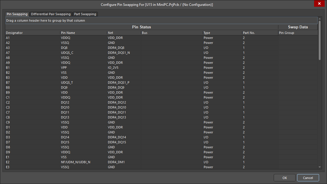
For each category of swapping, swap groups dictate what can be and what can not be swapped within a component. In the case of pin swapping, pins within a component that share a common pin group are able to be swapped with one another. Similarly for pair swapping and part swapping, it is the pair group and part group values that determine that a differential pair or sub part can be swapped respectively. The swap groups for a component are configured in the Configure Pin Swapping dialog, shown in the image below. It is accessible in the following ways:
- In a PCB document, right-click on the component then select Component Actions » Configure Pin/Part Swapping.
- In a schematic document, right-click on the component then select Part Actions » Configure Pin Swapping.
- In a schematic document, click the Configure Component button at the bottom of the Configure Swapping Information In Components dialog (Tools » Configure Pin Swapping).
- In a PCB document, click the Configure Component button at the bottom of the Configure Swapping Information In Components dialog (Tools » Pin/Part Swapping » Configure).
- Double-click on any of the components in the Configure Swapping Information In Components dialog.
Options and Controls of the Configure Pin Swapping DialogExpandCollapse
Pin Swapping Tab

The Pin Swapping tab
A component pin is swappable with another pin in that component when it belongs to the same pin group. Use this tab of the dialog to view and organize the pin groups for your component.
- Pin Status - lists the Designator, Pin Name, Net, Bus, Type, and Part No. for each pin. You can group the data to your preference or project requirements by dragging and dropping column headers into the Drag a column header here to group by that column region. You can also reorder the column headers by dragging them into a different horizontal order.
- Swap Data - lists the Pin Group information for each pin to be swapped. Double-click within the Pin Group column to rename the group.
Right-click Menu
- Show/Hide Columns - use to configure which columns are visible.
- Assign Pin-Swap Groups By - automatically assign pin swap groups by either Designator, Pin Name, Net, Bus, Type, Part No., Part Mode, or Pin Group. Select multiple pins before right-clicking in order to assign groups at the same time.
- Add To Pin-Swap Group - use to create new or add to existing pin-swap groups. New pin-swap groups are automatically named using numerical values (e.g., 1, 2, 3, etc.). You can add more than one pin at the same time by selecting multiple pins before right-clicking.
- Remove From Pin-Swap Group - use to remove the selected pin(s) from the pin-swap group. You can remove more than one pin at the same time by selecting multiple pins before right-clicking.
Differential Pair Swapping Tab

The Differential Pair Swapping tab
The swapping of differential pairs is governed by the value of the pair group for a differential pair. Use this tab of the dialog to view and organize the pair groups for your component.
- Pin Status - lists the Designator, Pin Name, Net, and Type for each pin. You can group the data to your preference or project requirements by dragging and dropping column headers into the Drag a column header here to group by that column region. You can also reorder the column headers by dragging them into a different horizontal order.
- Swap Data - lists the Pair Group information for each pair to be swapped. Double-click within the Pair Group column to rename the group.
Right-click Menu
- Show/Hide Columns - use to configure which columns are visible.
- Add To Pair-Swap Group - use to create new or add to existing pair-swap groups. New pair-swap groups are automatically named using numerical values (e.g., 1, 2, 3, etc.). You can add more than one pair at the same time by selecting multiple pairs before right-clicking.
- Remove From Pair-Swap Group - use to remove the selected pair(s) from the pair-swap group. You can remove more than one pair at the same time by selecting multiple pairs before right-clicking.
Part Swapping Tab
The Part Swapping tab
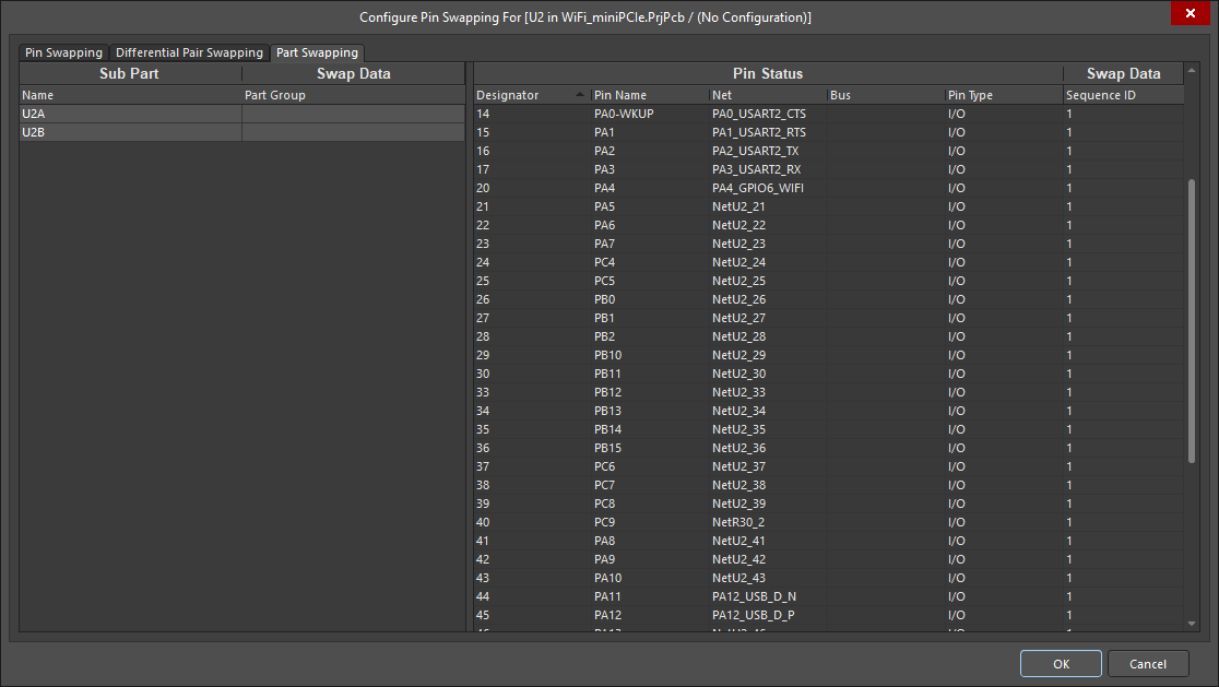
Part swapping for a component is configured with the part group and sequence ID attributes. The sequence ID attribute determines equivalence of the pins between swappable sub-parts. Use this tab of the dialog to view and organize the part groups for your components.
Right-click Menu
- Add To Part-Swap Group - use to create new or add to existing part-swap groups. New part-swap groups are automatically named using numerical values (e.g., 1, 2, 3, etc.). You can add more than one part at the same time by selecting multiple parts before right-clicking.
- Remove From Part-Swap Group - use to remove the selected part(s) from the part-swap group. You can remove more than one part at the same time by selecting multiple parts before right-clicking.
- Show/Hide Columns - use this to determine which columns are visible in the Pin Swapping tab of the dialog.
- Assign/Remove Part Sequence Number - the sequence ID attribute determines equivalence of the pins between swappable sub-parts. Create new or add to existing sequence ID groups. You can add/remove more than one part to a sequence ID at the same time by selecting multiple parts before right-clicking. New groups are automatically named using numerical values (e.g., 1, 2, 3, etc.). Double-click within the Sequence ID column to rename the group.
Pin Groups
A component pin is swappable with another pin in that component when it belongs to the same pin group (has the same pin group value). The pin group is an attribute of each pin in the component and its value can be any alphanumeric string. The pin groups for the entire component are set up in the Configure Pin Swapping dialog.
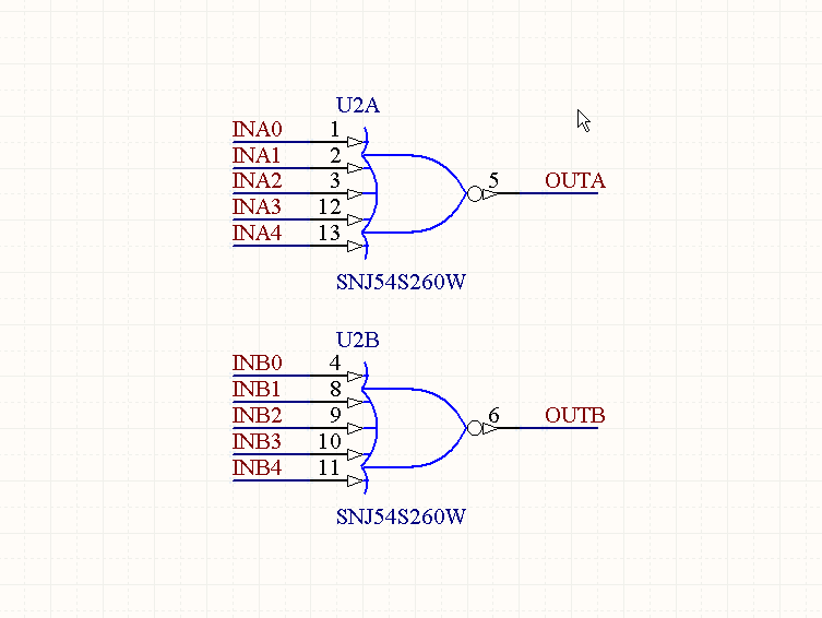 Schematic containing a Dual 5-Input Positive-NOR Gate component. Each of the input pins for either sub parts are logically equivalent and presenting an ideal situation for pin swapping.
Consider the schematic shown in the image above, which contains the two 5-Input NOR Gates for the SNJ54S260 component. Each of the nets, INA0 to INA4, can be swapped with each other due to the nature of the NOR Gate. Similarly, each of the nets INB0 to INB4 can be swapped, however a INAx net can not be swapped with a INBx net.
The swapping constraints for the NOR gate are defined in the Configure Pin Swapping dialog. Giving the nets INAx the swap group 1, and the nets INBx the swap group 2 ensures that swapping will only be performed by the system in such a way that it is consistent with the component logic. Leaving the Pin Group value for a pin empty denotes that the pin is unavailable for swapping.
Part Groups and Sequence IDs
It is common for a component to consist of multiple functionally equivalent subparts. Part swapping allows the nets of such equivalent sub-parts to be swapped. Consider again the component shown in the image above. Both NOR gates offer identical functionality and the nets (INA0, INA1, INA2, INA3, INA4, OUTA) are able to be swapped with nets (INB0, INB1, INB2, INB3, INB4, OUTB).
Part swapping for a component is configured with the part group and sequence ID attributes. These are both text attributes and are accessible in the Part Swapping tab of the Configure Pin Swapping dialog, as shown below. The image below also displays the part group and sequence ID settings corresponding to the component shown in the image above. The part group indicates which sub-parts are able to be swapped with one another. The two sub-parts are able to be swapped and consequently, in the image below, their part groups are given the same value of 1.
The sequence ID attribute determines equivalence of the pins between swappable sub-parts. In the NOR gate example it is important that the input pins are not interchanged with the output pins when a part swap occurs. The image below shows the sequence ID are set so that OUTA swaps with OUTB, INA0 swaps with INB0, INA1 swaps with INB1 and so on.
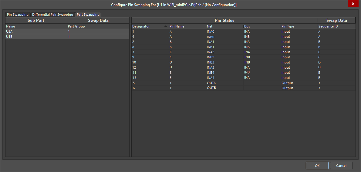 Setting up part swap groups in the Configure Pin Swapping dialog for a Dual 5-Input NOR Gate component.
Note that Part Swapping is only available for components designed as sub-parts as it is based upon swapping all the nets between two sub-parts.
Pair Groups
The swapping of differential pairs is governed by the value of the pair group for a differential pair. The pair group attribute is accessed in the Differential Pair Swapping tab of the Configure Pin Swapping dialog. There are three modes in the Differential Pair Swapping tab that can be set by accessing the drop down box in the lower left corner.
- Show Pairs From Directives - The system will use differential pair directives placed on the schematic to populate the differential pairs in the table.
- Show Pairs From FPGA - The system will use differential pair data obtained from FPGA information available to the component to pair up the pins. Note that this mode is available when the component is an FPGA.
- Show All Pins - The system will display all the component pins.
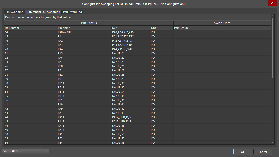 Setting up Pair Swap groups in the Configure Pin Swapping dialog.
Controlling How the Swaps are Performed on the Schematic
In the PCB editor pin, pair, and part swaps are performed by exchanging nets on component pads and corresponding copper. When the changes are merged into the schematics there are two ways that a pin swap can be handled, either by swapping the pins on the component symbol, or by swapping net labels on the wires attached to the pins. Each approach has its advantages and disadvantages.
Swapping the pins will always work on the schematic, but it may mean that this instance of the component symbol is no longer the same as it was defined in the library. In this situation it means the symbol cannot be updated from the library, and it also means that other instances of the same component in this design will have a different pin arrangement. Thus, this approach is ideal for simple components, such as a resistor arrays.
Performing the swap on the schematic by swapping net labels can only be done if the connectivity is established through the net labels, and if the pins are not hard-wired together. The advantage of this approach is that the component symbol does not change, and can be updated from the library at a later date. This approach is the best choice for a complex component, such as a FPGA, where physically moving two pins on the symbol could result in an I/O bank-based symbol presenting incorrectly.
You may determine how the swaps are performed by choosing the Adding / Removing Net-Labels or Changing Schematic Pins options in the Allow Pin Swapping Using these Methods section of the Project Options - Options dialog, as shown below.
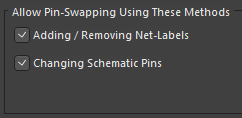 These project options govern how pin swaps are updated in the schematic documents.
Enabling Pin, Pair, and Part Swapping on the PCB
The swapping options for a PCB component can be configured in the Properties panel, which presents the properties for that component when it is selected in the design space. The options can be found in the Swapping Options region of the General tab.

Swapping options for PCB components can also be defined through the Configure Swapping Information in Components dialog, which lists all components used in the design (or library) with their current swap settings. When accessed from the PCB editor, the dialog includes an additional column for enabling/disabling swapping of each component on the board, called Enable in PCB.
The Configure Swapping Information in Components dialog can be accessed from the Schematic Editor, Schematic Library Editor, and PCB Editor, as follows:
- Schematic Editor/Schematic Library Editor - by choosing the Tools » Configure Pin Swapping command from the main menus.
- PCB Editor - by choosing the Tools » Pin/Part Swapping » Configure command from the main menus.
The swap group attributes needed to setup pin, pair and part swapping within a component are stored in the Schematic components. However it is the PCB editor where this information is used and each PCB component has an option to allow pin swapping of its pins. It can therefore be easier to use the dialog from the PCB Editor.
Use the Configure Swapping Information in Components dialog to quickly define swapping across components. The dialog includes a powerful right-click menu, making it very easy to quickly copy the settings from one component to another, or enable/disable multiple components in a single click.
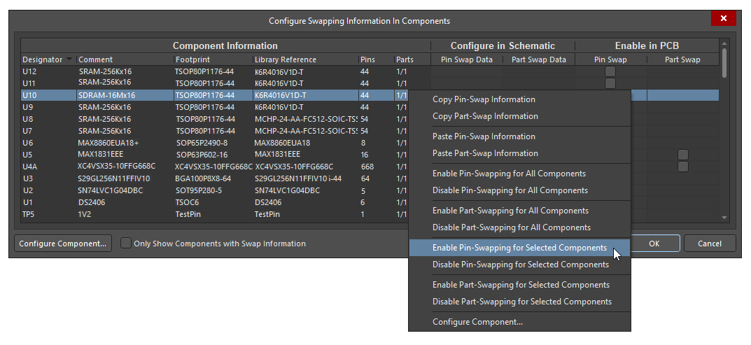 The Configure Swapping Information In Components dialog.
Options and Controls of the Configure Swapping Information in Components DialogExpandCollapse
- Component Information - displays all relevant information about the listed components: Designator, Comment, Footprint, Library Reference, Pins, and Parts.
- Configure in Schematic
-
Enable in PCB
If no check box is available, double-click the component to open the
Configure Pin Swapping dialog and configure its pin/part swapping settings under the
Pin Swapping and/or
Part Swapping tabs. The component must have assigned pin/part swapping groups in order for pin/part swapping to be enabled.
- Configure Component - click to open the Configure Pin Swapping dialog to configure swap settings for the pins and subparts of each component on the board.
- Only Show Components with Swap Information - check to only display components that have been configured to enable pin and/or part swapping.
Double-clicking on a component in the
Configure Swapping Information in Components dialog will open the
Configure Pin Swapping dialog for that component, where you can define the swap group settings for pins, differential pairs, and subparts with more control.
Performing Pin, Pair, and Part Swaps
Interactive Pin, Pair, and Part Swapping
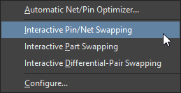
Interactive swapping allow pins, differential pairs, or subparts to be swapped one at a time in the PCB editor. The interactive swapping commands are found in the Tools » Pin/Part Swapping sub-menu (the Interactive Pin/Net Swapping, Interactive Differential-Pair Swapping and Interactive Part Swapping commands). Once the command is selected from the menu, everything in the PCB design space is masked (faded), except those entities that are swappable. Keep an eye on the Status Bar, it will prompt you for the next action. The steps required to perform a swap are displayed on the status line:
- The first step is to select one of the highlighted pins that will become the source of the pin swap. In the case of pair or part swapping, the differential pair or sub-part that the pin belongs to will be subsequently swapped.
- The second step is to select the target pin for the swap. For pair or part swapping, this pin will be representative of a differential pair or a sub-part.
The stages of interactively part swapping the Dual 5-input NOR gate component are shown in the two images below. There are two subparts that can be swapped, meaning each of their five pins can be selected, as shown in the image above. Pin 8 is selected corresponding to the subpart U2B. The system then highlights the pins of subpart U2A that can be swapped.
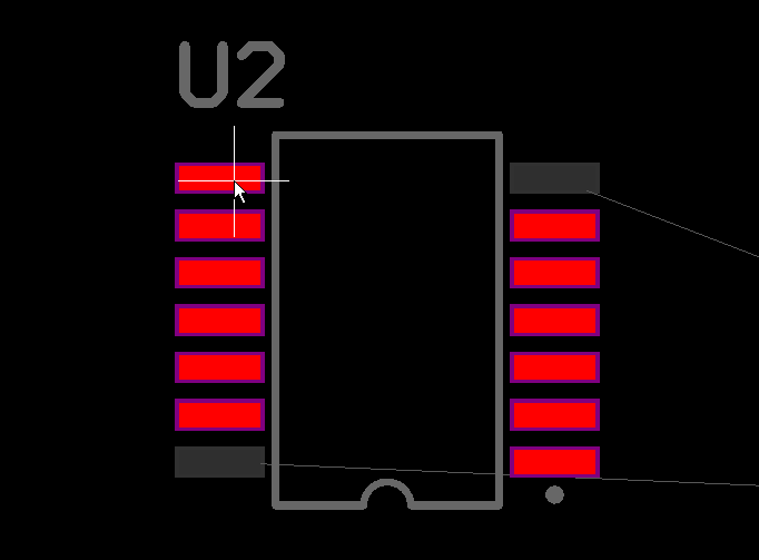
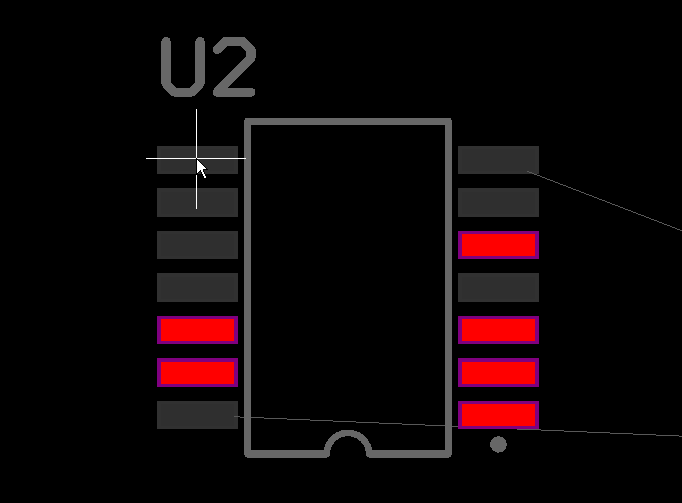 First image, step 1 - select a pin to be swapped, available pins will highlight. Second image, step 2 - select a target pin.
- It is not necessary to define Part Sequence values for differential pair pins, the differential pair definition details which is the positive pin in the pair, and which is the negative pin.
- Swap information will also appear in the Messages panel.
Automatic Pin/Net Optimizer
The Automatic Pin/Net Optimizer is a two-stage tool. Select Tools » Pin/Part Swapping » Automatic Pin/Net Optimizer from the PCB editor menu to perform an automatic optimization.
The Automatic Pin/Net Optimizer first runs a fast single-pass optimizer that attempts to minimize cross overs and connection lengths, but may actually increase them. When this is complete you will be asked if you want to run the iterative optimizer. The iterative optimizer will perform multiple passes in an attempt to reduce the number of cross overs and connection lengths.

Passing the Changes Back to the Schematic
When you configure the swap groups in the Configure Pin Swapping dialog the edits you make are immediately applied to the schematic components, regardless of which editor was active when the command was launched. However, design changes that are a result of you performing a pin, differential pair, or subpart swap in the PCB editor are propagated back to the schematic using the standard Design Update process.
Pushing the Changes from the PCB to the Schematic
Pin, pair, and part swaps are passed back to the schematic in the same way that other design changes are transferred - by selecting Design » Update from the menus. Depending on how the Allow Pin-Swapping options are configured in the Project Options - Options dialog, pin swaps will be performed as:
- Change Pin Names - this change will move the pins on the symbol. The pins are not actually moved on the symbol, but it will be visually apparent that the two pins have moved or swapping locations.
- Move Pins to Different Nets - this change will swap the net labels on the attached wires.
- Change Sub-Part ID - this change will change the sub-part index when a part swap is performed.
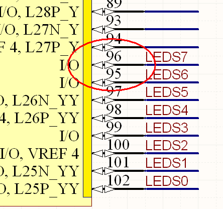
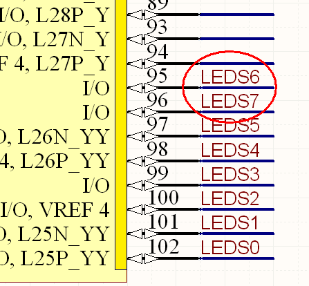
The first image shows a pin swap resolved in the schematic by swapping pins. The second image shows the swap resolved by moving the net labels.
If the schematic does not update to show swapped pins or parts, press the End key to refresh the display.
Taking Advantage of the New Pin/Part Swap System with FPGA Designs
Other than the obvious advantages that intelligent pin, pair, and part swapping provides, the ability to swap partially routed sub-nets brings a new dimension to swapping that is ideal for working with large capacity FPGAs. The dynamic net re-assignment allows you to use a multi-stage design process with progressively refined pin/net assignments
Initial I/O Assignment
In this stage, the FPGAs' and other device pins have their net assignments setup in whichever way is easiest at the schematic level. Usually, this means merely adding net labels in numeric bus order to the pins on the FPGA. The Smart Paste feature in the Schematic Editor is ideal for doing this.
Initial Connection Optimization
The design can be transferred to PCB layout, where there will be a lot of connection crossovers because of the random assignment at the schematic level. Running the Tools » Pin/Part Swapping » Automatic Net/Pin Optimizer command which uses pin and net information to dynamically re-assign nets and improve routability will quickly provide a large reduction in the number of crossovers. For example, the system can reconnect multiple BGA devices that have been escape routed on multiple layers of a PCB document. The result does not need to be ideal yet, as it is used to primarily make connections more visually manageable at the PCB level.
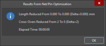
After launching the command, the Automatic Pin/Net Optimizer is run. This is a two-stage tool that first runs a fast single-pass optimizer that attempts to minimize cross-overs and connection lengths, but may actually increase them. When this is complete, you will be asked if you want to run the iterative optimizer. The iterative optimizer will perform multiple passes in an attempt to reduce the number of crossovers and connection lengths. The results of the optimization are displayed after the optimizer run completes.
Escape Routing
Fanout and Escape routing can now be performed on large devices on the PCB (right-click on the component to selectively perform fanout/escape routing). This may worsen the previously optimized assignments, but that does not matter at this point.
Escaped Connection Optimization
Run the automatic optimizer again. This time, it will take advantage of the pre-routed sections of fanout/escape routing.
Manual Routing
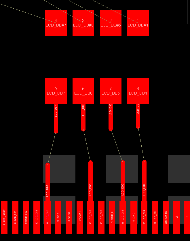
You can now treat the ends of the escape routes as 'targets' to route towards. Ignoring the actual connection lines, due to the fact that you can route from the other ends of the nets toward the nearest escaped I/O route (spatially and by layer) on the PCB, rather than the one that is on the same net. The connections will not line up. Instead, you will end up with a series of small gaps between the escape routing from the FPGA I/O pins, as well as your routing coming from other parts of the PCB. The image below shows a simple example of this.
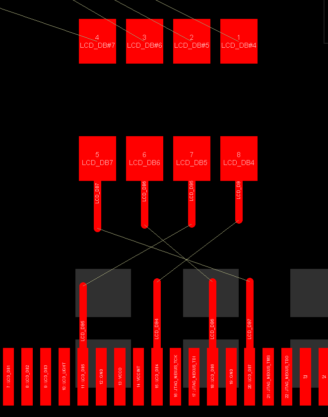
Final optimization
Run the automatic optimizer again and it will assign the routed subnets to the closest possible escaped I/O pin. This will leave you with a set of very short connections to complete. The automatic optimizer has special routines to produce a good result in this case. These can now be interactively or automatically routed.
Manual Pin Swaps
Use the interactive swapper to perform any specific pin swap changes that you need.
Propagate Changes Back to Schematic
When you are ready to propagate these pin assignments back to the schematic, it is a good idea to disable pin changes on the schematic symbols. This is because FPGAs are often presented as multi-part components, with each bank of pins being a separate schematic part. Moving pins from one part to another would result in these symbols becoming logically incorrect, as the bank symbol would include pins that did not belong in that bank. In this situation, performing pin swaps by changing net labels is the correct approach.
Repeat as Often as Required
This process can be run as many times as required, and at any time during the design process.