Constraint Manager:
Your Design, Your Rules
Explore highly detailed design rules, ensuring scalability and intricate management for even the most complex projects.
Elevate Design Precision
with Constraint Manager
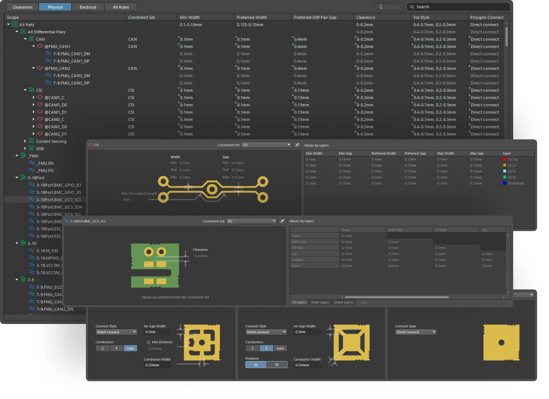
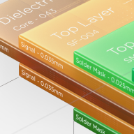
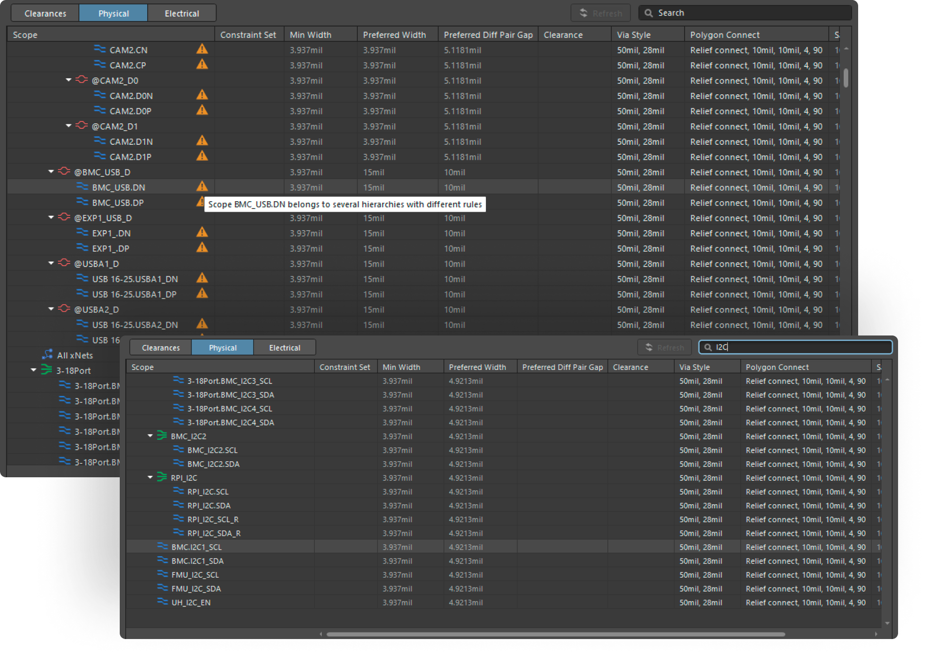
Efficient User Interface for Complex Designs
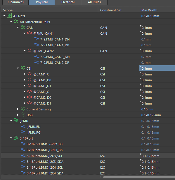
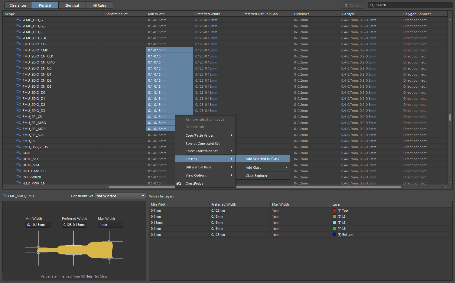
Dive into a user interface meticulously crafted to cater to intricate PCB designs. The structured layout ensures that even the most complex constraints are defined and managed with precision, optimizing your design process and elevating overall efficiency.
Experience Constraint Manager
in Altium Designer Today!
Trusted by over 20,000 companies
Key Capabilities
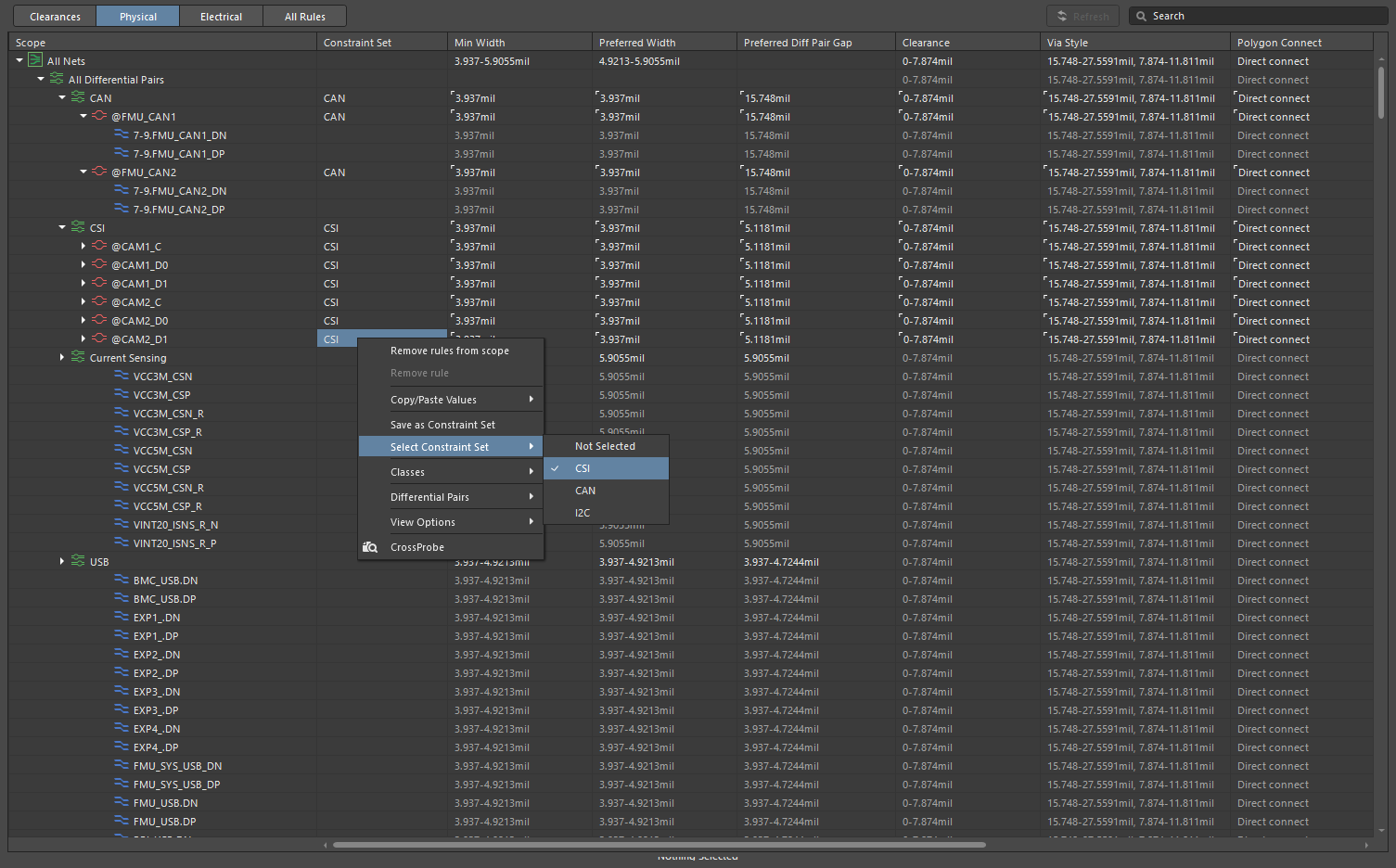
Reusable Constraint Sets
Maximize your design efficiency by creating and saving constraint sets that can be reused across your project. This not only ensures design consistency but also significantly reduces setup time for new projects.
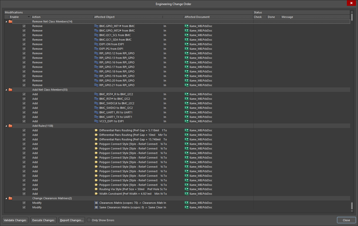
Schematic-to-Board Rule Transition
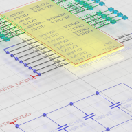
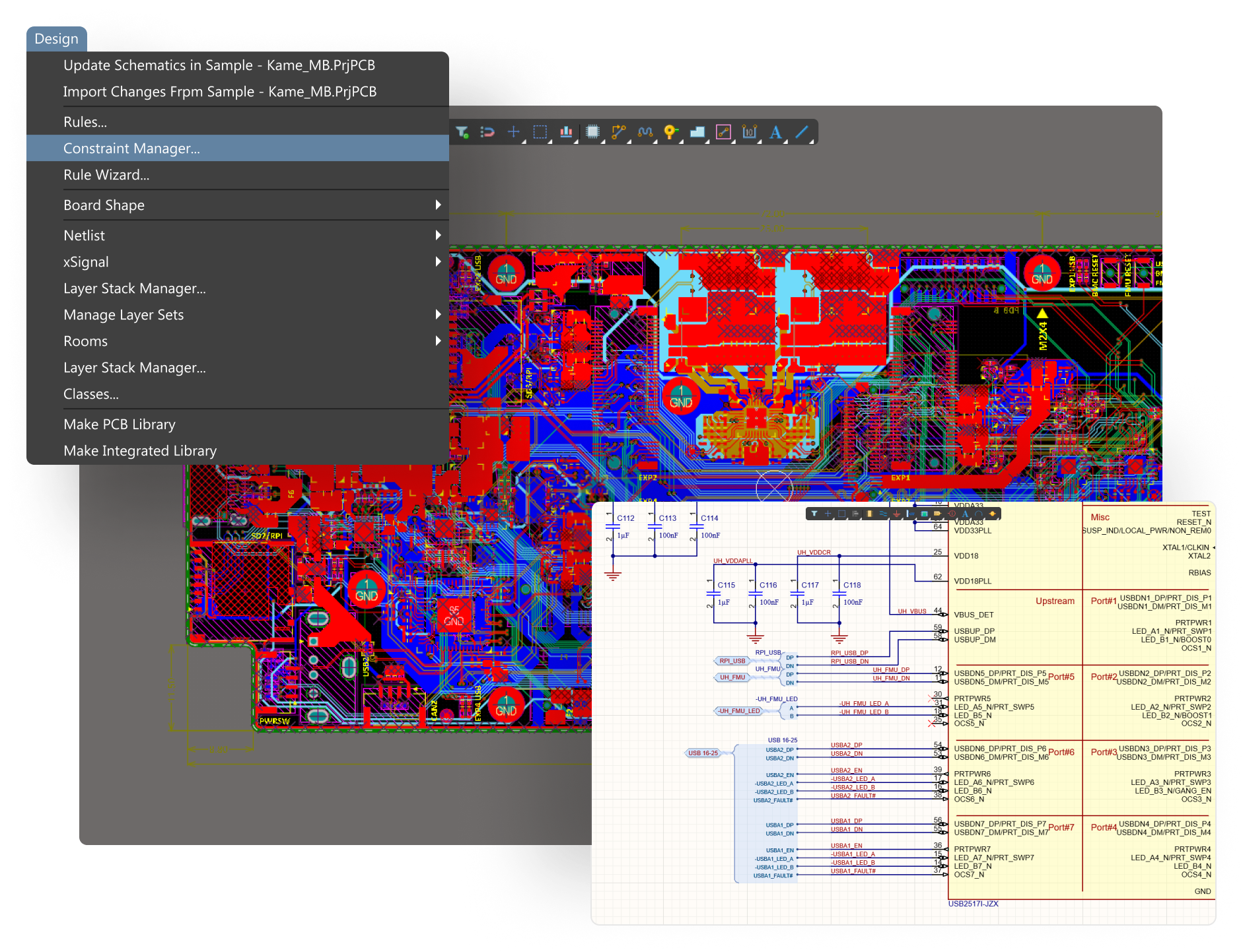
Maintain design integrity with seamless rule transitions from the schematic domain to the PCB layout. This ensures that every design rule defined in the schematic phase is accurately reflected and adhered to during PCB layout.
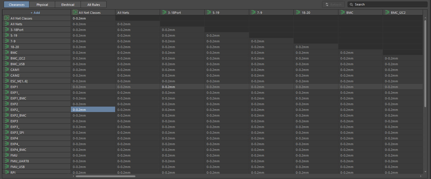
Class-to-Class Clearance Matrix
Achieve granular control over signal spacings with the Class-to-Class Clearance Matrix. Define specific clearance values between different net classes, ensuring optimal layout for reliability and manufacturability.
Easy Class and Differential Pair Grouping
Simplify your design process by effortlessly grouping components into classes or differential pairs. This not only streamlines rule assignment but also ensures that related components adhere to the same set of constraints.
Quick Filter Options
Navigate through your constraints with agility using quick search options. Instantly find and view specific rules or sets, making the management and modification of constraints a breeze.
Group Nets Rule Editing
Enhance productivity by editing multiple nets rule simultaneously. Whether it's adjusting values or changing rule priorities, batch editing ensures that large sets of rules are updated quickly and consistently.
Advanced xNet Grouping
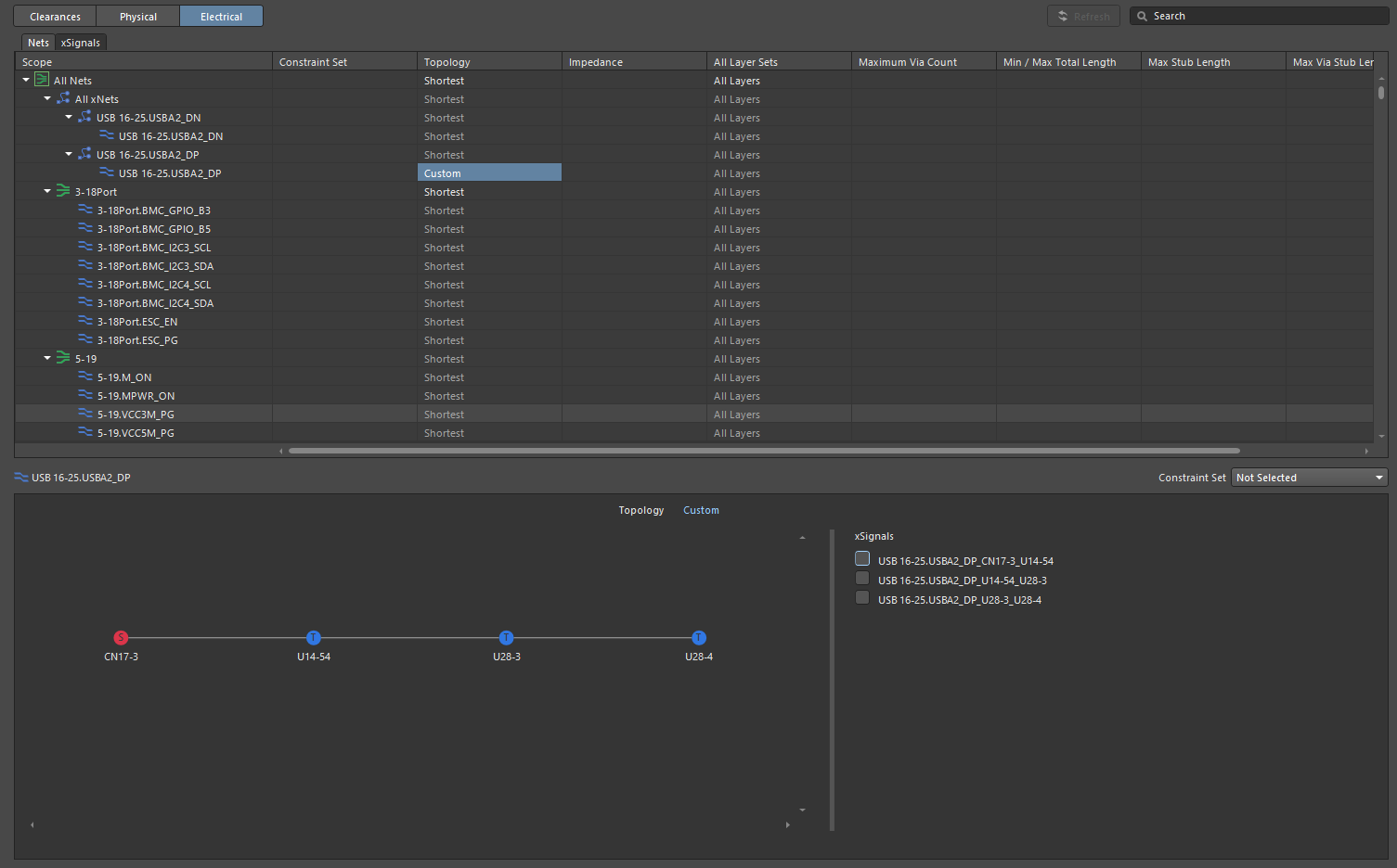
Manage intricate connection topologies with ease. By grouping multiple nets separated by discrete components, you can efficiently organize and maintain a clear structure in your designs, ensuring each component effectively transmits its designated signal.
Precise xSignal Path Definition
Master the intricacies of signal path design with precision. Harness the power to define length tolerances for each path between selected nodes. This meticulous attention to detail ensures your design perfectly aligns with the anticipated performance.

Start Your Free Trial Now
Accelerating PCB Design Through CoDesign of Multiple Designers
Explore Workflow Benefits
- Create a digital thread across domains and disciplines
- Enable digital management of processes and resources
- Enable stakeholders to monitor status and performance
- Maximize your return on your digital investments




%20copy%205.png)

.png)
.png)
.png)


